I feel like the rabbit in Alice in Wonderland who is always short on time…

Due to that, I may or may not be able to pack together a second Zen 4 part, that will depend on the launch coverage of it.
Nevertheless, I would like to share an interesting overview of the Zen evolution from Zen 1 to the upcoming Zen 4:

This image was mostly finished before Zen 4's official reveal at the end of August, but fate shut down Twitter in several countries so I couldn't publish it.
The upside is that some numbers that were previously unknown have been made public.
For example the RetiredEngineer® put a comparison table on Twitter, showing a couple of changes from Zen 3 to Zen 4.
Together with the CCD transistor count via Angstronomics and a few total guesses ( :> ) quite a bit of interesting data can be compared against each other.
Starting with Zen 1, we have a monolithic SoC design made by Global Foundries in 14/12 nm.
The chip size is about 212 mm² and integrates two 4-core CCX together with multiple I/O devices for PCIe, USB and the Infinity Fabric.
The transistor density for the whole SoC was at ~23 MTr/mm².
After that, AMD went for a chiplet design, manufacturing a Core Complex Die at TSMC’s N7 node, while the I/O functions (the PHYs scale little to none with a new node) were separated as a cheaper 12 nm die at Global Foundries.
With this change, we see a stark contrast when comparing both dies and the predecessor.
The 76 mm² core dies achieved 50 MTr/mm², 121% better transistor density compared to the monolithic design of Zen 1, while the I/O die is only at 16.72 MTr/mm², 26% worse than the Zen 1 SoC.
Zen 3 uses the “same” chiplet design and I/O die, but introduced new N7 CCDs with new CPU Cores, which were a bit larger, leading to a CCD size of ~ 84 mm² with basically the same transistor density.
The upcoming Zen 4 Raphael package is once again deploying the same chiplet design, but shrinking both chips with a new node.
The CCDs make the move from N7 to N5, achieving 91.3 MTr/mm², an increase of 83% compared to the predecessor.
If one would exclude the I/O PHYs and other analog components, it’s likely true that AMD achieved a 2x transistor density improvement vs. the previous node.
The new I/O die went from 12nm Global Foundries to 6 nm (N6) TSMC.
Even though the transistor shrinkage is massive, the new I/O die is pretty much as large as before.
There are a couple of potential reasons for that.
Analog devices, as they are used for I/O PHYs, do not scale well with new nodes.
The current 12 nm design already has all chip edges fairly well occupied with I/O.
One could redesign the PHYs to take less horizontal space and go further into the die, but this can be challenging and not desired.
If one would shrink down the current design, you probably would not make the chip smaller by any significant amount, as this design is pad (I/O PHY) limited.
What would shrink massively is the green portion in the middle, which would also lead to a lot of unused area.
However, you could integrate new features for “free”.
And this is what AMD has done, the I/O die now includes an RDNA2 iGPU with one WGP (128 Shaders) running at up to 2.2 GHz (~564 FP32 GFLOPs).
Enough to drive the display, simple applications and to capture a section of the business market, which previously was not accessible.
Besides the small iGPU, a VCN engine for video de/encoding will also be incorporated, together with a necessary display engine and its display PHYs.
Lastly, the 6 nm node should in general lead to better energy efficiency for the logic and SRAM devices.
In regard to the core design, AMD has always touched on several aspects with each generation
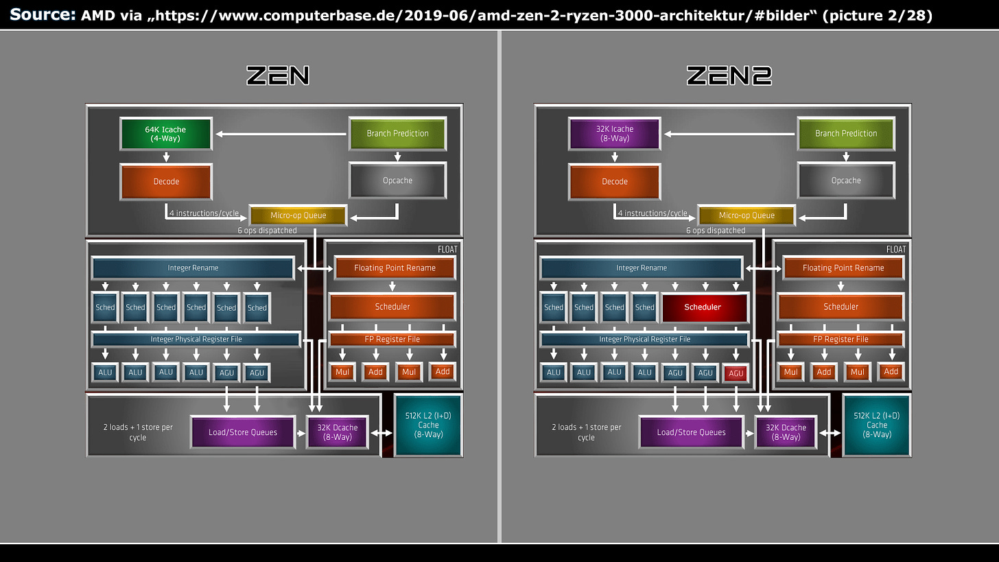
Zen 1 and 2 share the same microarchitecture foundation and as such are very familiar, using 4-core CCXes and logically a similar execution body.
But due to the 7 nm shrink, many structures on Zen 2 could be enlarged, some of them massively.
A new TAGE predictor has been added, branch target buffers have been (almost) doubled and the FPU width increased from 128 bits to 256 bits for single cycle AVX256 execution.
In addition, the L3 cache capacity per CCX was doubled.
It obviously goes on and on, for example multiple registers/buffers have been increased, like the re-order buffer to extract more ILP from the instruction stream, the Integer Register File got a few more entries and various scheduling queues for the execution units and load/store memory system.
Besides simple structure enlargements, AMD has rebalanced some aspects like the size of the L1 instruction cache and the op-cache capacity.
The company halved the L1I$ capacity to double the Op$ storage size, to source more
data from the latter, the more efficient and wider path, than the legacy L1I$/decode path.
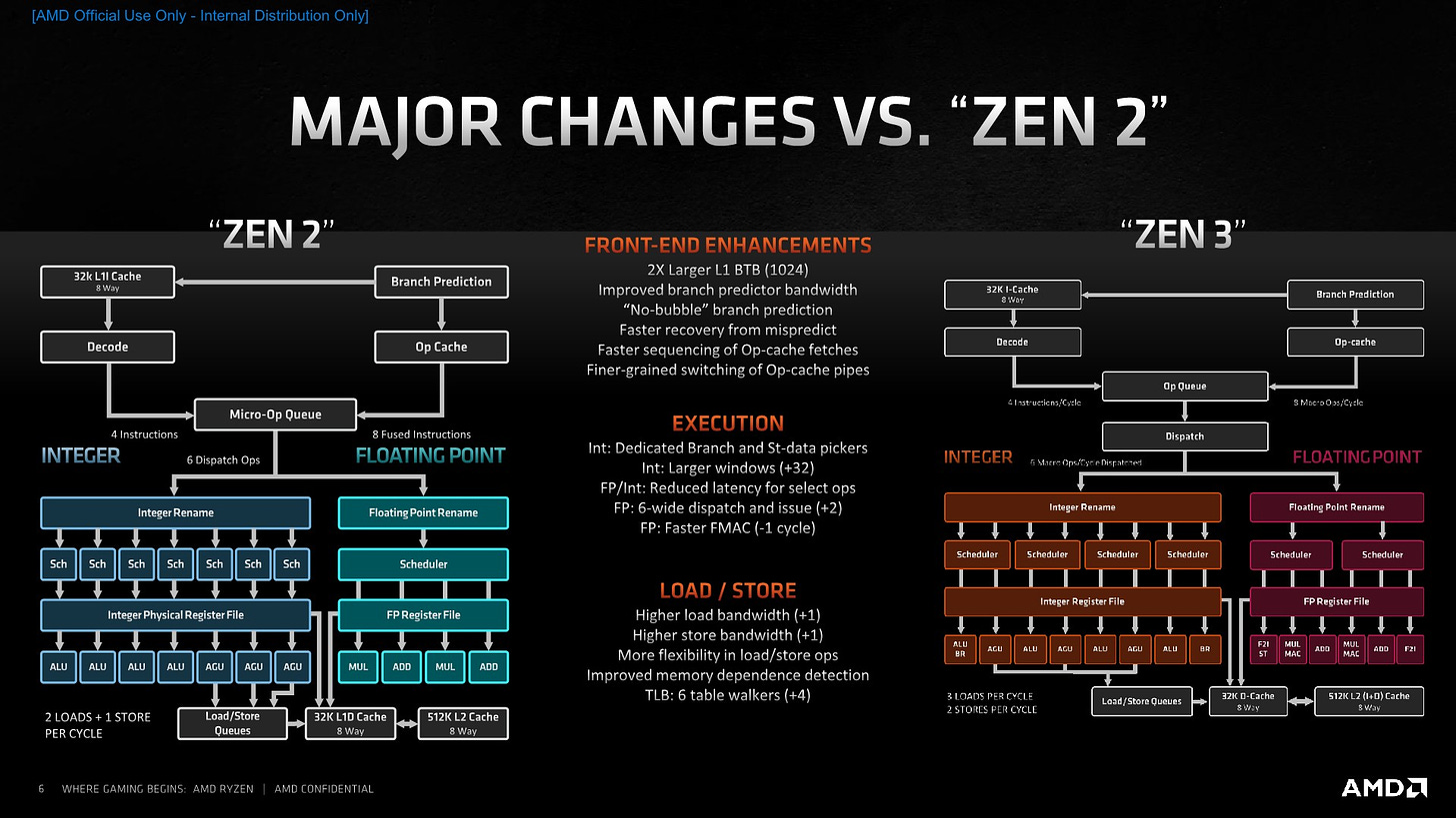
Zen 3 changed key aspects of the microarchitecture and set a new design foundation while using the same 7nm node.
Gone is the three level BTB structure in favor of just two levels with zero-bubble execution for the first level.
The execution body got wider and the port design was changed.
On a high-level you mostly see the expected scheme, several structure sizes have been slightly increased
Besides changing many core attributes, another highlight of Zen 3 was the change from 2x CCXes, with separate L3 caches and round-trips to the I/O die, to a single CCX design with a unified L3 cache structure serving all 8 cores.
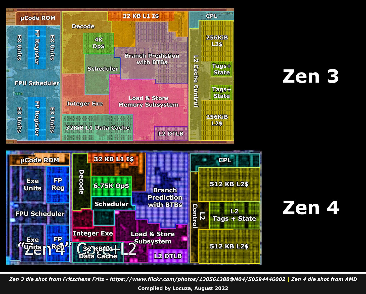
Zen 4 is pretty much a supercharged Zen 3 core, not unlike how Zen 2 was designed compared to Zen 1.
The same underlying microarchitecture is used while several structures are upgraded with the increased transistor budget of the 5nm process.
The width of the front-end was kept and follows us now since 4 generations.
As before, we have a 4-wide legacy decode path and a 6-wide dispatch to the execution engine.
However, the branch prediction part has always been improved and Zen 4 makes no exception here.
The BTBs have been increased yet again, and like with Zen 2, more emphasis has been placed on the Op$ path, increasing the capacity from 4K to 6.75K.
The execution body is the same as on Zen 3 previously (width + port design).
So we are still looking at 4x INT pipes, 3x AGUs and an FPU with 2x FADD and 2x FMUL(FMA) pipes (+ other pipes).
Similar to Zen 2, which poured a good chunk of its transistor budget into the FPU, Zen 4 again invests heavily in the FPU.
It’s now supporting AVX512 and a wide range of new instructions.
Moreover, for the first time after Zen 1, the amount of FP registers got increased by a decent amount.

As usual, you will also see many other structures being increased, like the re-order buffer holding now 320 entries (+25%).
In that regard, AMD is increasing that aspect still fairly conservatively, considering that Intel increased the ROB to 352 with Sunny Cove (from 224 on Skylake) and to a fairly massive size of 512 with Golden Cove.
With Zen 5 AMD will widen the front-end and potentially increase the ROB more aggressively, though the company will likely strive for a balanced point, keeping the perf/mm² high, as the generations before.
Well, relative to Intel one might say, it’s all relative.
::::::::::::::::::::::::::::::::::::::::::::::::::::::::::::::::::::::::::::::::::::::::::::::::::::::::::::::::::::::::::::::::::::::::::::::::::::::::::::::::::::::::::::::::
Subscribe for free to receive a newsletter when new content is available.
If you would like to support this work financially, you can choose the paid newsletter option or go to my Patreon page and select a tier that suits your budget - https://www.patreon.com/locuza
from Hacker News https://ift.tt/ZOGu3RW
No comments:
Post a Comment
Note: Only a member of this blog may post a comment.