Modern back-end web development is a large and complicated subject, and as someone who’s currently a few years into working professionally as a full-stack developer, I’m still struggling to understand some of the related concepts. Up until recently I didn’t fully grasp what microservices actually were on either a high or low level, and completing this course did a lot to demystify a lot about them for me.
The first thing I should say is that this course has a few general prerequisites even though it’s classed as “Beginner” level on Pluralsight, so it’s not the most ideal course for total beginners to web development in general. What should you already know (or have) for this course? I’d list these as necessary:
Some hands-on coding experience with both front-end (HTML, CSS, JavaScript) and back-end (in any language) web development
Ideally you should know how to code a front-end SPA in a modern library or framework (React, Vue, or Angular), along with a back-end API in a modern language & framework as well (JavaScript, Python, Ruby, C#, et al), even if both the front-end and back-end apps are only “Hello World”-level prototypes
Some exposure to at least 2 different frameworks from the same or different programming languages, to understand why you would want to use different frameworks or languages
Some knowledge of or exposure to DevOps (i.e Docker, Kubernetes, and CI/CD tools)
Some knowledge of or exposure to cloud services (AWS, Azure, or GCP)
Now if all of the above prerequisites sounds like a heady list, the primary reason I cite all of them is simply because this course puts all of those topics into context with each other, and more than that, also explains how they all fit together in the overarching theme of microservices. To this last point in particular, this is the only course of its kind that I’ve seen anywhere online that can help to get “beginners” up to speed on what they should know about microservices on a high level to prepare for the task of building them.
The breadth of content in this course spans a variety of topics from the high level to the low level, and without showing a single line of code, manages to explain and answer a lot of fundamental questions. These questions include what microservices are, the business case for microservices, how they’re built and architected together at a “bird’s eye” high level, and all of the implications of microservices, including Domain-Driven Design (DDD), data stores, data synchronization (i.e. messaging), Remote Procedure Calls (RPC), Cross-Origin Resource Sharing (CORS), gateways, authorization & authentication patterns & tools, load balancing, monitoring, logging, and much more. If you don’t know what any of these terms mean, it doesn’t matter, because the course explains all of them. Suffice it to say that it packs a huge amount of information and throws a bunch of things at you. This is why the course becomes especially helpful if you’ve already used some of the tools mentioned, in particular one of the cloud services (AWS, Azure, or GCP), and if you have some professional work experience in an agile team environment as well (because it goes into some detail about working in multiple teams across different layers of a product).
However, the truly exceptional quality of this course isn’t that it just throws a bunch of information at you, it also explains everything it mentions and puts all of the new information into context on visual diagrams to show where each piece fits. For example, if you didn’t know before the purpose of messaging (and the existence of tools like Akka, Kafka, or RabbitMQ), you will come away from the course with a basic understanding of what messaging is and what it’s used for. Similarly, if you didn’t know before what API gateways are, or how containers are used, or the point of load balancing, or what DevSecOps is, or what Elasticsearch is and what it’s used for, this course explains all of that as well, along with many other related topics.
Conclusion: To summarize this course, it’s easily the best introduction and overview to microservices that I’ve ever seen on any online platform and is an absolute must-do. While I’d recommend learning to actually code a simple back-end app first before doing this course, it’s definitely an essential primer to the topic of microservices for those just beginning on their journey to learning back-end web development. After having completed the course (just last month in April), I consider it not only one of the top courses on Pluralsight, but possibly THE best introductory course to the subject anywhere online, period.
W3W said that it was difficult to comment without the full details of what went wrong, but told the BBC: "We regularly check in with the emergency services that use the system to receive feedback. The overwhelming response is positive, and, time and time again we have been humbled to see stories where our technology has turned out to be life-saving.
A plan to reimagine math instruction for 6 million California students has become ensnared in equity and fairness issues — with critics saying proposed guidelines will hold back gifted students and supporters saying it will, over time, give all kindergartners through 12th-graders a better chance to excel.
The proposed new guidelines aim to accelerate achievement while making mathematical understanding more accessible and valuable to as many students as possible, including those shut out from high-level math in the past because they had been “tracked” in lower level classes. The guidelines call on educators generally to keep all students in the same courses until their junior year in high school, when they can choose advanced subjects, including calculus, statistics and other forms of data science.
Newsletter
The perils of parenting through a pandemic
What’s going on with school? What do kids need? Get 8 to 3, a newsletter dedicated to the questions that keep California families up at night.
You may occasionally receive promotional content from the Los Angeles Times.
Although still a draft, the Mathematics Framework achieved a milestone Wednesday, earning approval from the state’s Instructional Quality Commission. The members of that body moved the framework along, approving numerous recommendations that a writing team is expected to incorporate.
The commission told writers to remove a document that had become a point of contention for critics. It described its goals as calling out systemic racism in mathematics, while helping educators create more inclusive, successful classrooms. Critics said it needlessly injected race into the study of math.
The state Board of Education is scheduled to have the final say in November.
The new framework aligns with experts who say that efforts to fast-track as many students as possible to advanced math are misguided. And they see their campaign for a more thoughtful, inclusive pacing as a civil rights issue. Too many Latino and Black students and those from low-income families have been left behind as part of a math race in which a small number of students reach calculus.
“For a significant number of students, the rush to calculus can have a significant detrimental effect on the necessary deep-level understanding of grade-level mathematics to succeed in subsequent coursework, and districts should be aware of this research to make well-informed choices,” said Brian Lindaman, a member of the math faculty at Cal State Chico and part of a team of heavy hitters from academia who wrote the framework together.
“We are seeking to elevate students and to bring them up,” Lindaman said. “We’re not bringing anyone down. We’d like to bring everyone up.”
Opponents don’t see it that way, especially because the proposed guidance recommends doing away with the tracking of students, suggesting instead that students of all backgrounds and readiness should be grouped together in math classes through 10th grade.
For critics, this approach is a manifesto against calculus, high-achieving students and accelerated work in general.
“This is a disservice to all of our students,” Deanna Ponseti, a teacher at Warren T. Eich Middle School in Roseville, northeast of Sacramento, wrote in comments submitted to the commission.
“About half of my students come to me below grade level, and approximately 25% of them are more than two grade levels below,” she wrote. “Therefore a large portion of my time is spent teaching foundational skills to support the 6th grade curriculum. Even with differentiation, there is not enough time to have deeper level discussions and explore the depth of concepts for the 20% of our students that come to us well above grade level. At the same time, there is not enough time to meet the needs of those struggling students.”
A parent from Los Angeles called into the meeting to say that the new framework would create two classes of students, those learning at a slow pace in public schools, and those who could afford a more accelerated approach at a private school.
Most of the dozens of speakers during the public hearing were opponents — many of them identifying themselves as parents or teachers of gifted or high-achieving students.
But framework co-writer Jo Boaler, a professor in the Stanford Graduate School of Education, countered that research strongly supports the success of “heterogenous” classrooms. Another co-writer, Stanford assistant professor of education Jennifer Langer-Osuna, described a classroom of the near future where teachers would engage with students at all levels, so that everyone would feel challenged.
Calculus and other high-level math, they insisted, were not under assault.
State Sen. Ben Allen (D-Santa Monica), who sits on the commission, challenged whether that ideal was readily achievable in the typical California classroom. He also questioned the suggestion that tracking by math readiness was inevitably racist. He noted that in the Los Angeles Unified School District nearly all are students of color. So, he asked, how then would it be racist to track some L.A. Unified students into faster-moving coursework if they are ready for it?
He abstained on the vote forwarding the draft to the state Board of Education, emphasizing that he supports addressing past inequities while providing opportunity and deeper math understanding for all students.
State Board of Education President Linda Darling-Hammond said an underlying goal of the framework is simply to modernize math education.
“Part of what’s going on in the framework is an attempt to bring mathematics education into the 21st century, in terms of what kind of mathematics kids get opportunities,” Darling-Hammond said in an interview. “The old [way], the idea that calculus is the capstone, is one that originates with a committee of 10 men in 1892.”
A key element is elevating data science, which for many students is likely to be more valuable than calculus, added Darling-Hammond, who hasn’t yet had an opportunity to review the framework in detail.
Some of the opposition has focused on a document cited in the framework: A Pathway to Equitable Math Instruction. In an opinion piece for the Wall Street Journal, Williamson Evers, a former U.S. assistant secretary of Education, said the document was representative of a move toward subjective answers to math problems, watering down the curriculum and needlessly racializing the science of math.
“This program is quite a comedown for math, from an objective academic discipline to a tool for political activism,” he wrote.
In their work, the Pathway authors wrote, “Teachers must engage in critical praxis that interrogates the ways in which they perpetuate white supremacy culture in their own classrooms, and develop a plan toward antiracist math education.”
The commission ultimately followed the advice of the analysts from the state Department of Education, who counseled that they remove references to the Pathway tool kit.
The reason, they said, was that the Pathway material was still being revised close to the time of the meeting and the department had lacked sufficient time to fully vet the tool kit in its final form.
This post is reconstructed from notes I wrote down in early February back when I did most of the work, so the information might be slightly out of date. I did my best in keeping them up to date and re-tested the firmware builds at the time of writing this post to make sure they all work as intended.
Serial console is one of the most important ways of communicating with embedded Linux systems. I’ve used a lot of USB serial adapters over the years, but they all seem to have two major drawbacks that are difficult to overcome:
They are not electrically isolated. Whenever I power up my target boards, there is always a small chance that a power surge will happen due to ground loop interference, which causes my connection to be interrupted on power-up:
FATAL: read zero bytes from port
term_exitfunc: reset failed for dev UNKNOWN: Input/output error
By the time I could reconnect with my terminal software (picocom in this case), I would have already missed a lot of critical messages printed by the bootloader. This makes diagnosing and debugging bootloader related problems very unpleasant. To make matters worse, should something bad happens to my board and a high voltage was sent to the tx/rx pins, it can potentially go back to my computer and destroy my PCH, since EHCI/XHCI controllers are typically integrated in the PCH nowadays.
The UART cable length limit makes it difficult to work with on a messy desk, as I would always need a USB hub or at least an extension cable, further contributing to the clutter, and the bare PCBs have risks of being accidentally sorted out by my other metallic tools if not careful.
While talking to some network engineers, I found that some people had Wi-Fi or BLE based wireless console adapters, which allow them to access the RS-232 serial consoles wirelessly. Some research later, a series of products called Airconsole from Cloudstore Limited perked my interests. From the looks of it, most of their Wi-Fi enabled options look extremely similar to a series of older “3G router” products manufactured by HAME. The Mini model looks almost identical to MPR-A5, the Std/Pro one looks almost identical to MPR-A1, and the XL looks almost identical to MPR-A2. These HAME models are later cloned by other manufacturers and then sold as generic products, and they can still be found to this day on places such as eBay and AliExpress.
With this information in mind, I figured it’s easier for me to make my own wireless serial console adapter with some of the old portable routers I have lying around. I have no need for Bluetooth connectivity or smartphone apps, all I want is something that I can connect to locally and lets me interact with a serial console over a secure connection. Transport security is highly desirable because I don’t want my login credentials to be transmitted in plaintext, not even on my own LAN.
After some consideration, I have decided running picocom over an SSH session, on a battery powered OpenWrt device would be the easiest to implement for me. SSH is the best option for me because the “trust on first use” design has a much lower setup overhead compared to a traditional PKI based TLS/HTTPS setup, while still remaining secure. OpenWrt offers an easy-to-use configuration web interface for setting up the Wi-Fi connection, has (mostly) up to date userspace software, and is pretty much the only Linux distribution that will work on these routers anyway.
Here are some alternatives solutions and ideas I have considered or found in my research, and why I did not pick them for this project:
esp-link: While being very affordable, it offers no transport security.
consrv: Go binaries are statically linked and too large for the extremely limited amount of storage space available, plus running yet another SSH server while I already have dropbear (provided by OpenWrt by default) feels very redundant.
Bluetooth based solutions have very limited range, and they are typically much more difficult to work with in general.
Proprietary 433MHz/2.4GHz off the shelf serial bridges often have fixed bitrates and lack proper transport encryption.
While not being wireless, if only electrical isolation is desired, digital isolators such as the ADUM3201 are widely available. The problem with this solution is now eight wires in total would be required, instead of the typical three, since vcc from both sides are needed for the digital isolator to function correctly.
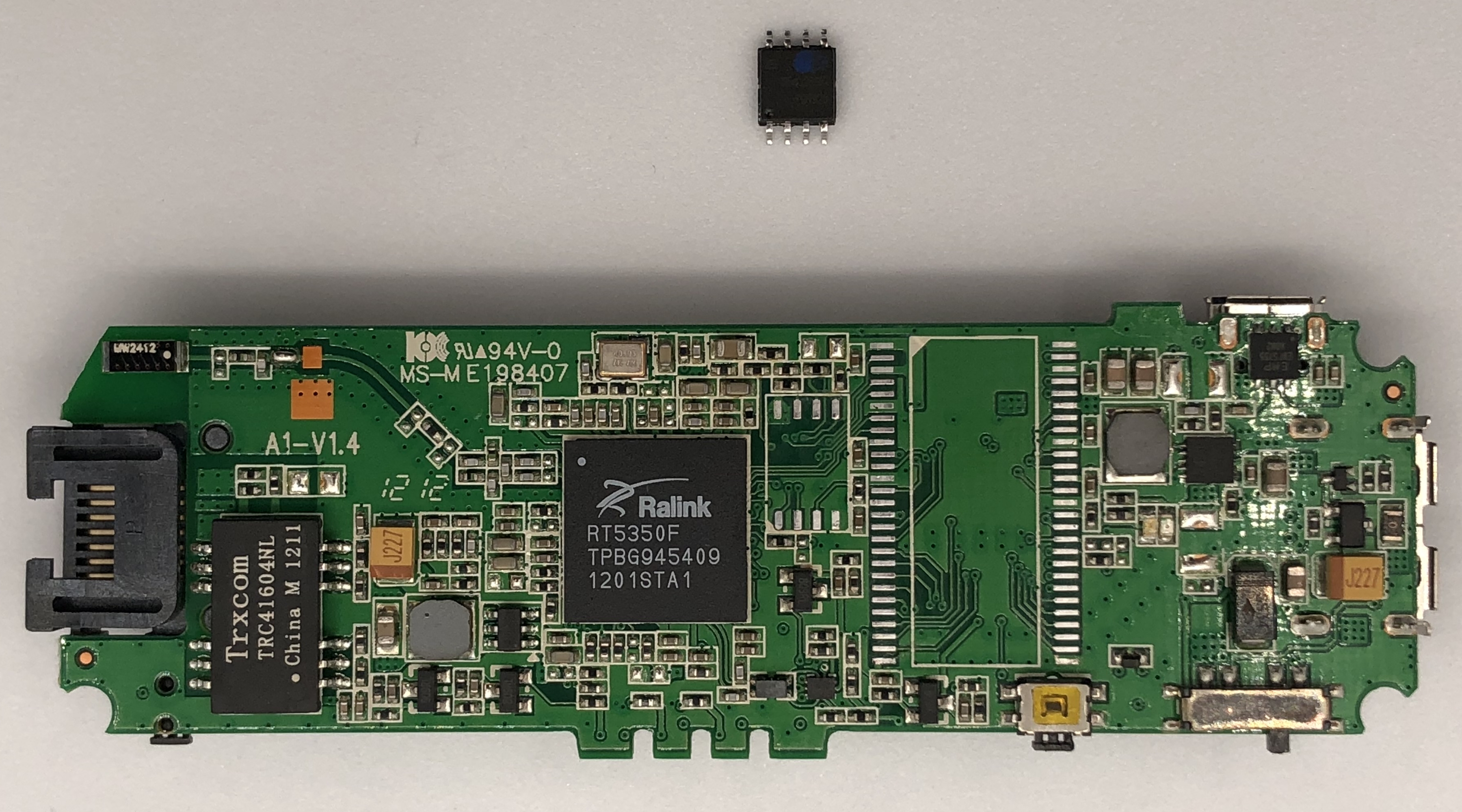
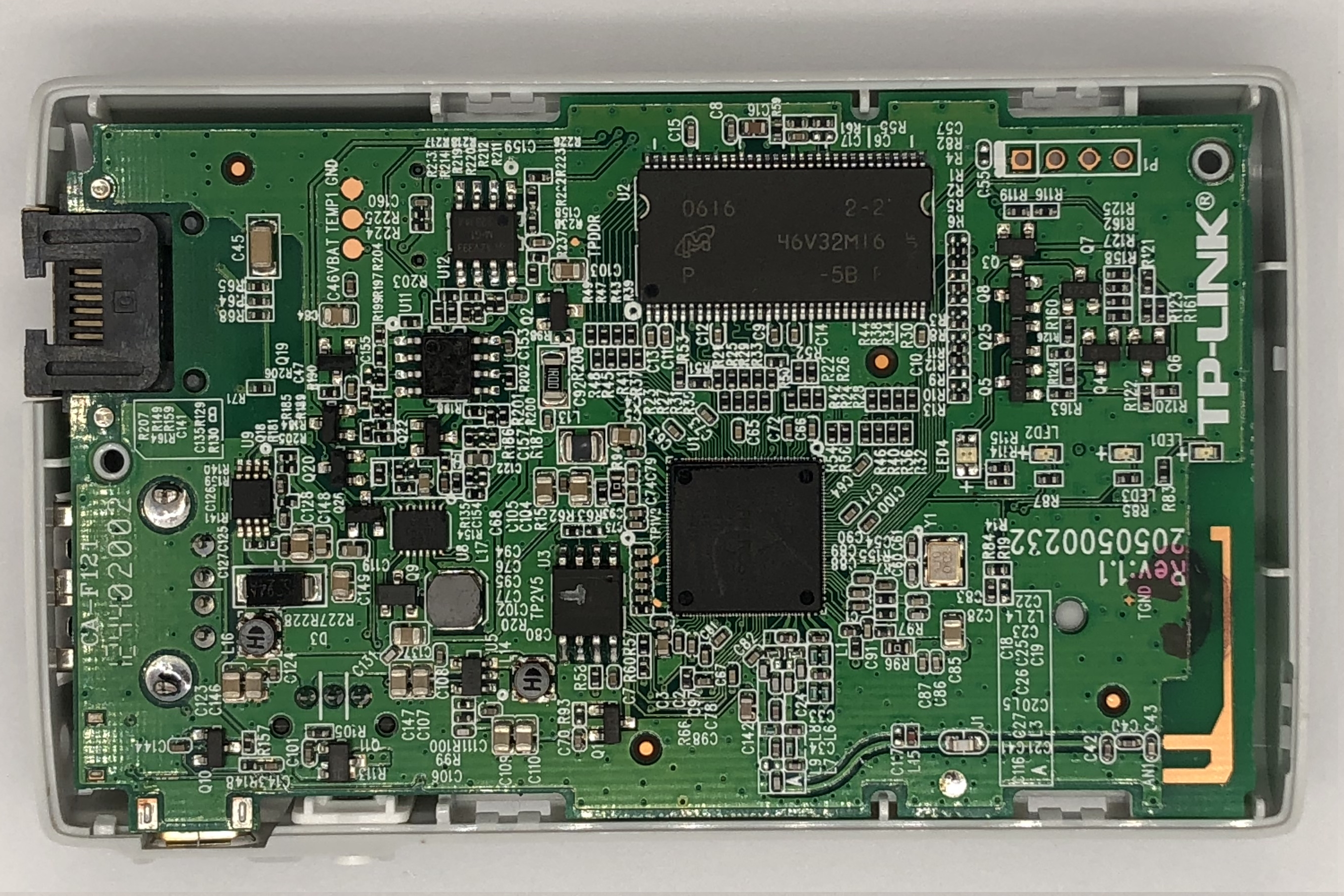
With the context out of the way, some hardware upgrades are required for me to be able to fit modern OpenWrt onto these devices I have. The TP-Link TL-MR11U only has 4MB of NOR flash and 32MB of DRAM. While 32MB is sufficient for what I’m going to run, 4MB is not enough to store the required software anymore. The HAME MPR-A1 only has 4MB of NOR flash and 16MB of DRAM, neither of which are sufficient for anything I need.
The MPR-A1 and the MPR-A2 are almost identical devices aside from having less storage, memory and a smaller battery. In fact OpenWrt builds for A2 will work on the A1 if you upgrade its NOR flash and DRAM. I’ll be putting in 8MB of NOR flash and 32MB of DRAM to match the MPR-A2. Disassembling the MPR-A1 was fairly straightforward, so I won’t post images here, as it bogs down the article.
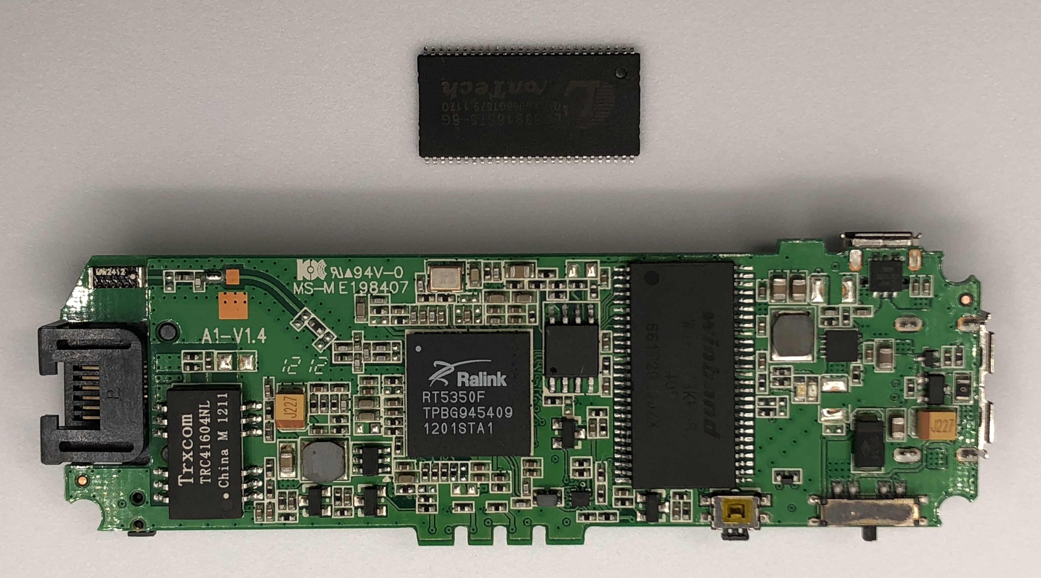
The new NOR flash was not soldered back until I spliced the firmware and wrote the new firmware image to the flash. Board images are all placed here for the sake of better organization.
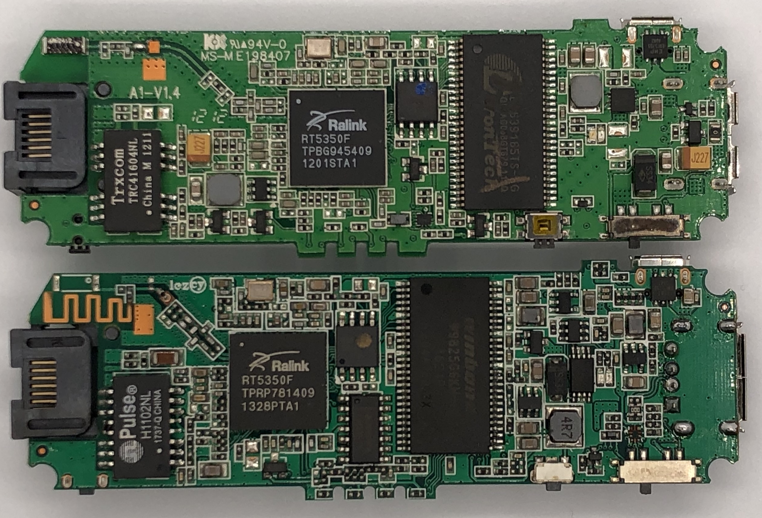
I just happened to have an MPR-A2 clone, so I thought I’d put the two PCBs together as a comparison too. It’s interesting to see the clone opted for cheaper parts in some places to cut costs. I won’t be working on the clone as it already has 8MB of NOR flash and 32MB of DRAM.
Top: genuine MPR-A1 | Bottom: MPR-A2 clone
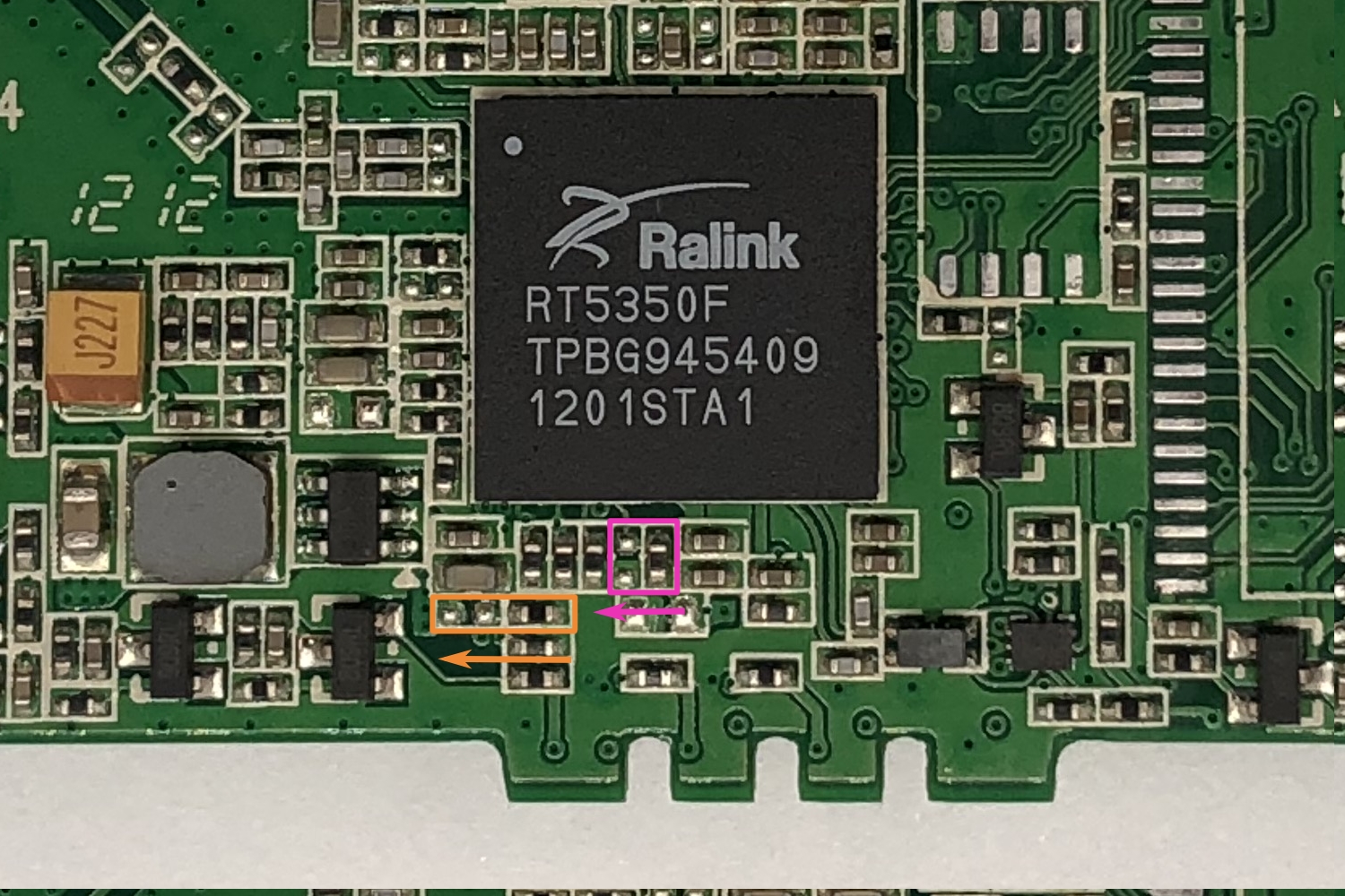
According to the RT5350F’s datasheet, DRAM configuration is either set in EEPROM, or configured externally via two bootstrapping pins. In MPR-A1’s case, it’s configured via those two bootstrapping pins. Unfortunately, this SoC cannot properly address one single 64MB DRAM chip (only 32MB*2), so 32MB is as good as it gets.
Bootstrapping pin configurations from the RT5350F datasheet.
MPR-A1's board with DRAM and NOR flash removed.
Bootstrapping pins on the PCB. Moving these two resistors to the left flips both bits, from 01 (16MB) to 10 (32MB).
Board after the DRAM and NOR flash have been upgraded and bootstrapping pins have been reconfigured.
For the MR11U, upgrading is much easier, since the bootloader can auto-detect the DRAM configuration and there are no bootstrapping pins to worry about. The datasheet of the SoC says the maximum supported flash size is 16MB, and the maximum supported DRAM size is 64MB, so that’s what I put in.
The upgraded PCB after some cleanup.
I won’t go over the setup process here, the wiki does a pretty good job explaining that. After the source has been cloned, I did the following to build my firmware image:
# check out the v19.07.7 branch
$ git checkout v19.07.7
# clean, update and force install all package feeds# -f is required because some packages won't show up as they contain files that may # override built-in packages, and this behavior is typically disallowed by default
$ scripts/feeds clean && scripts/feeds update -a && scripts/feeds install -af
This is the configuration I used for the upgraded MPR-A1. Since I’m borrowing the config for the MPR-A2, no further changes to the source code is required, as the new flash I put in matches the capacity of the MPR-A2. The change in DRAM will get picked up by the bootloader and passed onto the kernel thanks to the new bootstrapping configuration. On top of the defaults, I only enabled ECC and compression support in dropbear, added some USB serial drivers, picocom, shadow-utils (because I need to add a user to the device) and LuCI (the web configuration interface).
CONFIG_TARGET_ramips=y
CONFIG_TARGET_ramips_rt305x=y
CONFIG_TARGET_ramips_rt305x_DEVICE_mpr-a2=y

CONFIG_DEVEL=y
CONFIG_CCACHE=y

# enable ECC and compression support in dropbear
CONFIG_DROPBEAR_ECC=y
CONFIG_DROPBEAR_ECC_FULL=y
CONFIG_DROPBEAR_ZLIB=y

# enable luci
CONFIG_PACKAGE_luci=y

# USB serial drivers
CONFIG_PACKAGE_kmod-usb-acm=y
CONFIG_PACKAGE_kmod-usb-serial=y
CONFIG_PACKAGE_kmod-usb-serial-ch341=y
CONFIG_PACKAGE_kmod-usb-serial-cp210x=y
CONFIG_PACKAGE_kmod-usb-serial-ftdi=y
CONFIG_PACKAGE_kmod-usb-serial-pl2303=y

# terminal software
CONFIG_PACKAGE_picocom=y

# enable shadow_utils
CONFIG_PACKAGE_shadow-utils=y
After writing these to .config in the root directory of the source tree, simply running make defconfig will tell the build system to automatically resolve dependencies and complete the config file.
$ make defconfig
# download all of the required source archives
$ make download -j10
# compile the image, running with a high nice value to avoid stalling other applications on the system
$ nice -n 19 make -j$(nproc)
Unfortunately, the build quickly failed. Running make V=s -j1 revealed the problem originated from build_dir/host/mklibs-0.1.35, whose makefile is tools/mklibs/Makefile.
In file included from elf_data.hpp:24,
                 from elf.cpp:21:
elf.hpp:52:56: error: ISO C++17 does not allow dynamic exception specifications
   52 |       const section &get_section(unsigned int i) const throw (std::out_of_range) { return *sections.at(i); };
      |                                                        ^~~~~
elf.hpp:62:47: error: ISO C++17 does not allow dynamic exception specifications
   62 |       static file *open(const char *filename) throw (std::bad_alloc, std::runtime_error);
      |                                               ^~~~~
elf.hpp:65:38: error: ISO C++17 does not allow dynamic exception specifications
   65 |       file(uint8_t *mem, size_t len) throw (std::bad_alloc) : mem(mem), len(len) { }
      |                                      ^~~~~
elf.hpp:68:52: error: ISO C++17 does not allow dynamic exception specifications
   68 |         static file *open_class(uint8_t *, size_t) throw (std::bad_alloc, std::runtime_error);
      |                                                    ^~~~~
elf.hpp:131:55: error: ISO C++17 does not allow dynamic exception specifications
  131 |         std::string get_string(uint32_t offset) const throw (std::bad_alloc)
      |                                                       ^~~~~
elf.hpp:266:39: error: ISO C++17 does not allow dynamic exception specifications
  266 |       std::string get_version() const throw (std::bad_alloc);
      |                                       ^~~~~
elf.hpp:267:44: error: ISO C++17 does not allow dynamic exception specifications
  267 |       std::string get_version_file() const throw (std::bad_alloc);
      |                                            ^~~~~
elf.hpp:269:44: error: ISO C++17 does not allow dynamic exception specifications
  269 |       std::string get_name_version() const throw (std::bad_alloc);
      |                                            ^~~~~
elf.hpp:308:29: error: ISO C++17 does not allow dynamic exception specifications
  308 |       version_requirement() throw (std::bad_alloc);
      |                             ^~~~~
----------snip----------
make[7]: *** [Makefile:382: elf.o] Error 1
I checked what the upstream Makefile looks like on 21.02, and it seems like I need HOST_CPPFLAGS += -std=gnu++98 in my makefile. Further inspection reveals that the 0.1.35 version does not even exist on Debian’s server anymore, so I upgraded the version number, archive extension (.xz instead of .gz) and the hash corresponding to v0.1.44 as well.
After deleting build_dir/host/mklibs-0.1.35 and re-running the build process, everything worked out this time, and I was able to generate a system image at bin/targets/ramips/rt305x/openwrt-ramips-rt305x-mpr-a2-squashfs-sysupgrade.bin. I’ll put that aside for now and compile an image for the TP-Link device.
For the TP-Link TL-MR11U, a little modification to the source is required. The upgraded DRAM does not require any changes since it’s auto-detected by the bootloader and then passed onto the kernel, but for the flash size, I need to change the build target of this device to make sure I used a 16MB flash layout. For the old ar71xx target, it’s as simple as changing which macro this device’s definition points to. My hardware revision is v2, but the v2 definition points to v1, so it’s v1 that I would need to change.
This is very important for the ar71xx target, much more important than the previous device, which was rampis, as I will elaborate in the firmware splicing part below.
The ar71xx target has now been dropped due to it being mostly replaced by the newer, device-tree based ath79 target. However, not all devices have been ported to ath79.
The configuration is very similar to the previous device:
CONFIG_TARGET_ar71xx=y
CONFIG_TARGET_ar71xx_tiny=y
CONFIG_TARGET_ar71xx_tiny_DEVICE_tl-mr11u-v2=y

CONFIG_DEVEL=y
CONFIG_CCACHE=y

# enable ECC and compression support in dropbear
CONFIG_DROPBEAR_ECC=y
CONFIG_DROPBEAR_ECC_FULL=y
CONFIG_DROPBEAR_ZLIB=y

# enable luci
CONFIG_PACKAGE_luci=y

# USB serial drivers
CONFIG_PACKAGE_kmod-usb-acm=y
CONFIG_PACKAGE_kmod-usb-serial=y
CONFIG_PACKAGE_kmod-usb-serial-ch341=y
CONFIG_PACKAGE_kmod-usb-serial-cp210x=y
CONFIG_PACKAGE_kmod-usb-serial-ftdi=y
CONFIG_PACKAGE_kmod-usb-serial-pl2303=y

# terminal software
CONFIG_PACKAGE_picocom=y

# enable shadow_utils
CONFIG_PACKAGE_shadow-utils=y
Now to build the firmware:
# complete configuration
$ make defconfig
# clean built artifacts
$ make clean
# download all of the required source archives
$ make download -j10
# compile the image, running with a high nice value to avoid stalling other applications on the system
$ nice -n 19 make -j$(nproc)
Now I have the image at bin/targets/ar71xx/tiny/openwrt-ar71xx-tiny-tl-mr11u-v2-squashfs-factory.bin.
Splicing and flashing firmware
First, I read both chips I took off from the devices with my programmer and flashrom. The flash programmer I used is an excellent open-source project: stm32-vserprog. The repository has both hardware and firmware designs. This can read and write chips much faster than the CH341 based programmers, and it’s quite easy to assemble.
These two devices are both MIPS, but that’s pretty much where the similarities end. The firmware setup for these two devices are completely different, so I needed to take different approaches to splice things together and put back onto the new NOR flash.
Generally speaking, a wireless router/access point type embedded Linux system like this would have a couple of partitions:
bootloader (u-boot in both devices mentioned here)
bootloader environment variables (optional, sometimes stored within the bootloader partition)
RF calibration data for the Wi-Fi radio (MAC addresses are commonly stored here too)
kernel
rootfs (typically read-only)
overlay (where the user configuration is saved, and mounted as overlay on top of the read-only rootfs)
It’s worth noting that wireless calibration data must be preserved, because this is unique on a per-board basis. This is why cross-flashing other people’s full flash dumps as-is is typically not a good idea, because you will end up with subpar RF performance and wrong MAC addresses, not to mention potentially violating FCC (or the local equivalent) regulations, and why it’s always recommended having a full image backup of the flash before tinkering with any devices.
First, I need to cut up the stock firmware dump to individual partition images according to the partition table for use later. This can be simply accomplished with dd if=A1_full_dump.bin of=$PARTITION_NAME bs=1 count=$SIZE_IN_BYTES skip=$START_OFFSET_IN_BYTES, or simply selecting, copying and pasting data in a hex editor.
So overall the only two partitions I need from the original flash image would be u-boot-env and factory. u-boot-env contains configuration for the bootloader that I don’t need to modify, factory is the conventional radio calibration data and MAC address storage partition for Ralink (and MediaTek MIPS) devices.
The sysupgrade image I got from the build system is actually a complete uImage directly bootable by the bootloader, with the rootfs squashfs image appended after it. All I need to do is writing this to 0x50000 of the flash. This sysupgrade file does have some trailing metadata, but these will be automatically erased when the overlay partition is automatically reformatted on first boot, thus it can be safely ignored.
$ file bin/targets/ramips/rt305x/openwrt-ramips-rt305x-mpr-a2-squashfs-sysupgrade.bin
bin/targets/ramips/rt305x/openwrt-ramips-rt305x-mpr-a2-squashfs-sysupgrade.bin: u-boot legacy uImage, Linux Kernel Image, Linux/MIPS, OS Kernel Image (lzma), 1280356 bytes, Mon Feb 15 15:22:37 2021, Load Address: 0x80000000, Entry Point: 0x80000000, Header CRC: 0x2D529961, Data CRC: 0x804D50B5
Now that I have all the data, it’s time to reconstruct a bootable full flash image. While this could have been more convenient to do in a GUI hex editor, I thought it would be easier to explain what’s going on if I did it with dd. The firmware partition of MPR-A2 is 0x7b0000 in size instead of 0x3b0000, but otherwise they have identical flash layouts.
# Take the modified bootloader binary that can use 32MB of DRAM, and generate a padding to pad it to 0x30000 with 0xFF.
$ FILE="uboot256.img" dd if=/dev/zero bs=1count=$((0x30000 -$(stat --format=%s $FILE)))|tr \\000\\377 > u-boot_padding
91104+0 records in
91104+0 records out
91104 bytes (91 kB, 89 KiB) copied, 0.0971852 s, 937 kB/s
# Concatenate the padding with the u-boot image
$ cat uboot256.img u-boot_padding > u-boot_partition
# Concatenate the u-boot partiton (now with the correct size), u-boot environment variable partition the wireless calibration data parition together.
$ cat u-boot_partition u-boot-env factory > header
# Generate a padding filled with 0xFF to pad the frimware partiton to the correct size
$ FILE="openwrt-ramips-rt305x-mpr-a2-squashfs-sysupgrade.bin" dd if=/dev/zero bs=1count=$((0x7b0000 -$(stat --format=%s $FILE)))|tr \\000\\377 > firmware_padding
3865866+0 records in
3865866+0 records out
3865866 bytes (3.9 MB, 3.7 MiB) copied, 1.49983 s, 2.6 MB/s
# Concatenate the sysupgrade image with the padding
$ cat openwrt-ramips-rt305x-mpr-a2-squashfs-sysupgrade.bin firmware_padding > firmware_partiton
# Concatenate everything together
$ cat header firmware_padding > full.bin
# Write the assembled full image to the new flash chip
$ flashrom -p serprog:dev=/dev/ttyACM1:400000000 -w full.bin
With the chip written, I soldered it back. After cleaning up the board, I powered it on and the system came up as expected. Took about 3 minutes to fully initialize the jffs2 overlay as it needed to erase everything in the overlay partition. Subsequent normal boots take about 1 minute, while being a little slow, is still an acceptable trade-off for the convenience.
[   78.870911] jffs2_scan_eraseblock(): End of filesystem marker found at 0x0
[   78.926935] jffs2_build_filesystem(): unlocking the mtd device...
[   78.927077] done.
[   78.943362] jffs2_build_filesystem(): erasing all blocks after the end marker...
[   80.627250] br-lan: port 1(eth0) entered blocking state
[   80.652812] br-lan: port 1(eth0) entered disabled state
[   80.663982] device eth0 entered promiscuous mode
[   80.838653] br-lan: port 1(eth0) entered blocking state
[   80.849204] br-lan: port 1(eth0) entered forwarding state
[   80.860561] IPv6: ADDRCONF(NETDEV_UP): br-lan: link is not ready
[   82.058579] IPv6: ADDRCONF(NETDEV_CHANGE): br-lan: link becomes ready
[  177.313272] done.
[  177.317307] jffs2: notice: (1135) jffs2_build_xattr_subsystem: complete building xattr subsystem, 0 of xdatum (0 unchecked, 0 orphan) and 0 of xref (0 dead, 0 orphan) found.
[  177.746829] overlayfs: upper fs does not support tmpfile.
This device requires a different approach. Since the factory bootloader can auto-detect the 64MB of DRAM I put in, and I can simply apply openwrt-ar71xx-tiny-tl-mr11u-v2-squashfs-factory.bin from the stock TP-Link firmware, all I really needed to do was mirroring the ART (Atheros Radio Test, wireless calibration data) partition to where it should be on a 16MB device. On these Atheros based devices, ART is commonly simply located in the last 64KB of the flash, and this device is no exception.
Doing this one with dd would be slightly more difficult than the previous one and would require more messy arithmetic operations, so I didn’t bother with this one and simply used a hex editor to do the job. Basically, the gist is:
Create a new 16MB file filled with 0xFF
Open the original 4MB flash dump and copy it to the beginning of the 16MB file in overwrite mode
Copy the last 64KB of the original flash dump to the last 64KB of the new 16MB file in overwrite mode
After I have the 16MB OpenWrt image flashed onto the device, it will automatically pick up the new ART data I placed at the end of the new 16MB flash. Now all I need to do was writing this image to the new 16MB chip and soldering it back to the board.
# Write the assembled full image to the new flash chip
$ flashrom -p serprog:dev=/dev/ttyACM1:400000000 -w full.bin
This board came up and finished erasing the overlay slightly faster than the other device, only taking a little over 2 minutes to initialize the overlay. Just like the previous device, normal boots take about 1 minute, while being a little slow, is still an acceptable trade-off for the convenience.
[   90.206076] jffs2_scan_eraseblock(): End of filesystem marker found at 0x0
[   90.211744] jffs2_build_filesystem(): unlocking the mtd device...
[   90.211818] done.
[   90.219575] jffs2_build_filesystem(): erasing all blocks after the end marker...
[   90.859188] br-lan: port 1(eth0) entered blocking state
[   90.870509] br-lan: port 1(eth0) entered disabled state
[   90.876126] device eth0 entered promiscuous mode
[   90.927039] IPv6: ADDRCONF(NETDEV_UP): br-lan: link is not ready
[   94.978202] eth0: link up (100Mbps/Full duplex)
[   94.981345] br-lan: port 1(eth0) entered blocking state
[   94.986506] br-lan: port 1(eth0) entered forwarding state
[   95.026917] IPv6: ADDRCONF(NETDEV_CHANGE): br-lan: link becomes ready
[  136.089805] done.
[  136.090335] jffs2: notice: (1205) jffs2_build_xattr_subsystem: complete building xattr subsystem, 0 of xdatum (0 unchecked, 0 orphan) and 0 of xref (0 dead, 0 orphan) found.
[  136.393070] overlayfs: upper fs does not support tmpfile.
I wrote a simple shell script that prints the current driver used and then calls picocom with one of the two possible serial adapter device nodes it finds. This can be set to a user’s login shell, so I won’t have to specify long commands when connecting to the device over ssh.
#!/bin/sh
OPTION1=/dev/ttyUSB0
OPTION2=/dev/ttyACM0
DEFAULT_BAUDRATE=115200if[ -c "$OPTION1"];thenADAPTER=$OPTION1elif[ -c "$OPTION2"];thenADAPTER=$OPTION2elseecho"No serial adapter found."exitfiecho"Using $ADAPTER at $DEFAULT_BAUDRATE baud."echo"Driver: $(basename $(readlink /sys/class/tty/$(basename $ADAPTER)/device/driver))"echo -e "Press [C-b] to change the baudrate. \n"exec /usr/bin/picocom --send-cmd '' --receive-cmd '' -b $DEFAULT_BAUDRATE$ADAPTER
After setting up the root password and wireless credentials, I copied my script to /usr/bin/serial_terminal to the device with scp and did some basic setup over SSH.
# set the script to executable
chmod +x /usr/bin/serial_terminal
# add a user called "uart" in the dialout group, whose login shell is my serial terminal script
useradd -g dialout -d /home/uart --create-home --shell /usr/bin/serial_terminal uart
# set a secure password for the "uart" user
passwd uart
# add new "shell" to the list of allowed shellsecho"/usr/bin/serial_terminal" >> /etc/shells
# add all of the files midified so far to sysupgrade.conf so they persist through factory resetsecho"/etc/shells" >> /etc/sysupgrade.conf
echo"/usr/bin/serial_terminal" >> /etc/sysupgrade.conf
echo"/home" >> /etc/sysupgrade.conf
Unfortunately, I was not able to get public key ssh authentication working properly on 19.07. Setting PubkeyAcceptedKeyTypes +ssh-rsa with ECC keys or switching to RSA keys silenced send_pubkey_test: no mutual signature algorithm from my client, but dropbear is always giving me authpriv.warn dropbear[1759]: Pubkey auth attempt with unknown algo for 'root' from xxx no matter what I tried, so I didn’t investigate further and thought dropbear on here is simply too old.
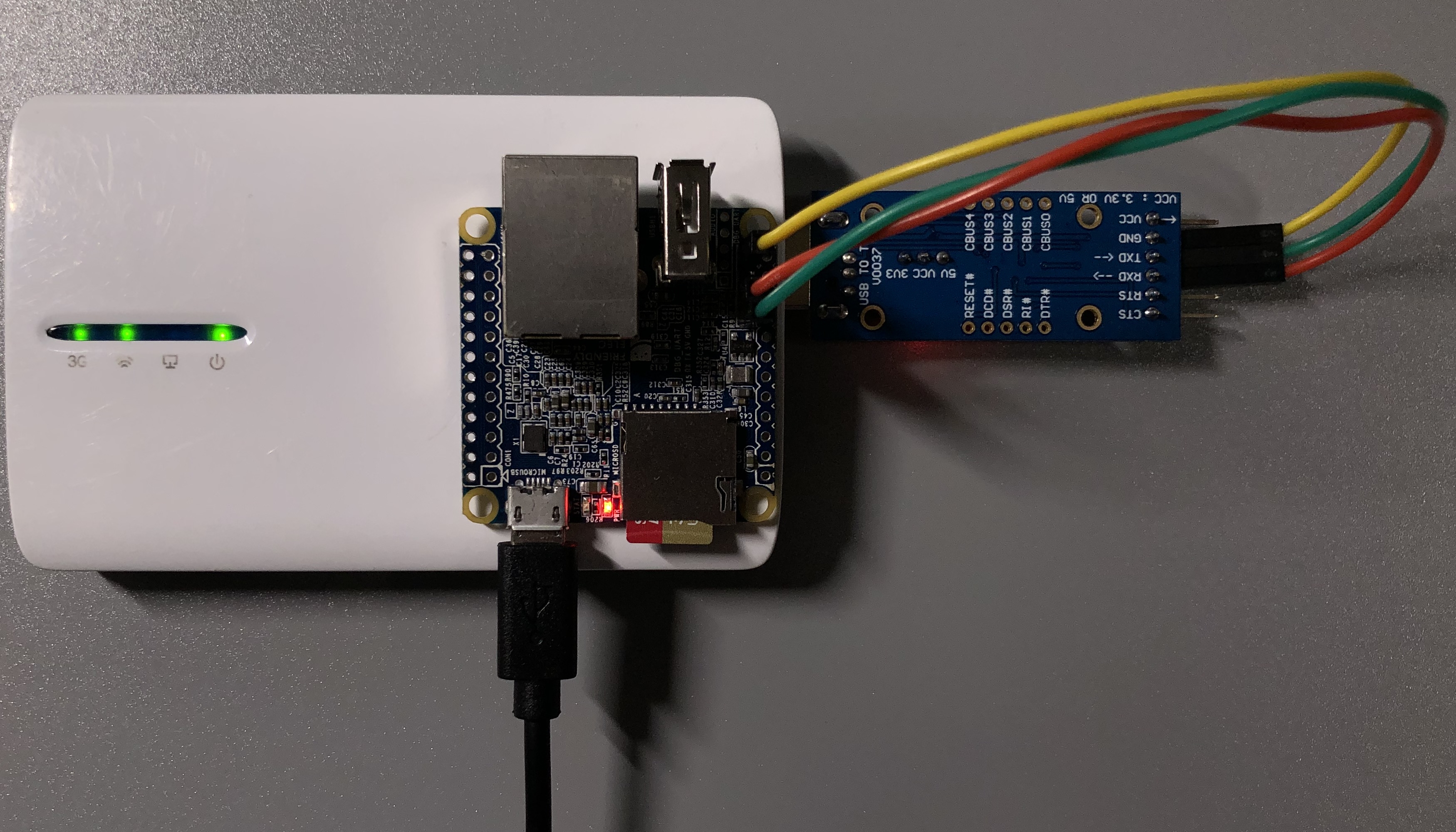
After everything has been set up, this is the final result. All of these devices are functionally identical as far as the use case is concerned, so there is only one demo. I connected to the device over ssh, powered up the target board connected to the serial adapter, and then ran htop to demonstrate psuedo-GUI applications mostly work pretty well here.
Testing setup with the TL-MR11U.
The MPR-A2 clone and the genuine MPR-A1 with serial adapters attached.
Apologies for the lack of playback control, I have not yet found any way to add playback control widgets for animated SVG.
Adding Bluetooth serial capabilities. While I don’t have much use for this feature, I can see it being useful for other people.
Forwarding the raw character device over SSH instead of running picocom on the remote. ttcssh will do what I want, but setup seems very convoluted for a non-essential feature, so I didn’t feel like setting this up here.
Upgrading to OpenWrt v21.02 and hopefully fix SSH public key login.
Brood X is emerging across 15 states. Here's how to decode all that buzzing from the trees.
(Inside Science) -- When you first hear it, a cicada chorus may sound like simple buzzing. But to a cicada, that cacophony is full of meaning.
There are three species in Brood X, the cohort of 17-year cicadas now emerging in much of the eastern U.S. Members of each species congregate with their own kind and talk to each other with their own species-specific sounds. Males sing to court females and "jam" the songs of other males, while females make clicks with their wings to encourage or repel suitors.
Humans can learn to decode these sounds. John Cooley, a biologist at the University of Connecticut, can speak cicada so well he can seduce insects of either sex. He uses his voice to imitate males and gentle finger snaps to imitate females.
"All the females are cueing in on is the pitch and the rhythm," he said. "You hit that, and you're going to get a response."
Males "sing" by vibrating tymbal organs located on the sides of the abdomen. They also produce alarm calls when handled, as seen in this video by Greg Holmes.
Loud or soft?
Cicadas spend most of their lives as juveniles called nymphs, living underground and feeding on fluid from tree roots. Eventually, they dig to the surface, shed their nymphal exoskeletons, and fly into the trees to sing, breed and die.
Most species don't synchronize their emergence; instead, a small batch will come out to breed every year. Such species are often called annual cicadas, even though they may live for several years as nymphs.
A male annual cicada will find his own spot from which to sing, and interested females who hear the song will fly to meet him. The louder the male's song, the farther it will travel, and the more females he can call in. As a result, the songs of annual species are often deafeningly loud.
Male annual cicadas like this Neocicada hieroglyphica must call in females from far away, so their songs are often deafeningly loud.
The songs of periodical cicadas, including the 17-year cicadas, sound loud en masse, but each male's song is typically quieter than that of an annual cicada. That's because periodical cicadas emerge on the same schedule, waiting for a set number of years and then all coming out to breed at once. The adults gather in dense choruses with huge numbers of individuals, so there's little point trying to call in females from far away. Instead, periodical cicada males use their songs to get the attention of females that are already nearby.
"It's obvious where the females are. They're right here in this giant pile of bugs," said Cooley. "The chorus is such an acoustical mess anyway, your sound's only going to travel a very short distance before it's washed out in the general chaos."
High or low?
The three species now emerging in Brood X -- Magicicada septendecim, M. cassini and M. septendecula -- have the longest documented lifespans of any cicadas in the world, according to Floyd Shockley, an entomologist with the Smithsonian National Museum of Natural History in Washington. Different regions have their own broods that emerge in different years, but all broods containing those three species are on 17-year schedules.
Females only want to mate with males of their own species, and songs are how they tell the difference. Species that emerge together in the same brood typically have songs that are easy to tell apart.
In Brood X, M. septendecim's song is low and haunting, resembling "a UFO landing or a strange musical note in the woods," said David Marshall, an evolutionary biologist with the University of Connecticut. M. cassini's is similar to M. septendecim's in structure, but higher and faster. M. septendecula has a more complicated song made up of rapid pulses that change tone half way through.
In the early 2000s, Cooley and Marshall discovered a previously unknown cicada species that appears to have changed its song to avoid being mistaken for its neighbors. While they can't be sure how the new species arose, evidence suggests the process started when some of the 17-year M. septendecim switched to a 13-year schedule. Marshall suspects the split happened at least several thousand years ago.
In the northern edge of its range, the new species, dubbed M. neotredecim, doesn't encounter any similar-sounding species, and it retains the song of its 17-year ancestors. But farther south, it meets another closely related 13-year species, M. tredecim, which sounds almost the same. In areas where M. neotredecim and M. tredecim emerge together, the new species appears to have shifted to a higher pitch. Evidently, the females' need to identify their own species was so strong that it drove males to evolve from baritones to tenors.
To click or not to click?
For a long time, the courtship rituals of cicadas in the Magicicada genus appeared to make little sense. The males would go through an elaborate series of songs and behaviors, while the females, to all appearances, "just sat there like lumps," said Cooley.
What was missing was a signal by the female to show she approved of a male's efforts. Researchers in the late 70s failed to spot it, and so did Marshall during his first field season in 1991. But four years later, Cooley and Marshall noticed what the male cicadas had been watching for all along: a flick of the female's wings that produced a soft click.
This wing-flick signal means "yes, come mate with me" -- but only if done at precisely the right time. Performed at any other time, it means "go away, I'm not interested."
To make matters worse, nearly all the wing-flicks one sees are of the "go away" variety, because females typically mate only once. By the time most researchers spotted the "come hither" wing-flick, they had already seen so many of the other kind that they'd learned to discount it.
"The females that you see obviously out in the chorus are the ones that are either not yet ready to mate, or they have already mated, and so they're not interested in mating," said Cooley. "They come into sexual receptivity unpredictably and gradually, and then they flick their wings, and boom, they're out of the mating pool."
Because mating opportunities are so rare, males will pursue anything that seems even vaguely promising. If a random movement or clicklike sound occurs at the right time, a male may mistake it for a receptive female.
"They'll try to mate with acorns. They'll try to mate with spiders. Anything," said Cooley. This was fortunate for the researchers, because it allowed them to perform experiments by snapping their fingers and posing miscellaneous objects as model cicadas. The caps of Sharpie pens worked well, being about the same size and color as a female cicada. So did an old light switch, which had "plenty of places on it where the male can attach his genitalia," said Cooley.
This video by Greg Holmes shows courtship and mating in Magicicada tredecim, a 13-year species that is very similar to M. septendecim.
The experiments confirmed how the wing-flick signals work, which in turn unlocked the whole process. A hopeful male will give a call, which for most Magicicada species consists of a sustained note that falls in pitch at the end. Then he will pause, watching and listening for a potential partner. If no one replies, he'll continue searching through the throng, often flying a short distance before trying again.
When a female does signal approval, the male will approach her, shifting to a faster series of calls with little pause in between. If another male tries to court the same female, the first male may sing over top of his rival's call, preventing the female from hearing the down-slurred ending that would entice her to reply.
When the male reaches his intended, he extends a tentative foreleg that often vibrates gently as he touches her. Then, if she allows it, he will climb aboard, shifting to a staccato song that lacks the down-slur. He keeps crooning until his body connects with hers.
Editor's note (May 28, 2021): This article was edited after publication to clarify when David Marshall believes the species M. septendecim and M. neotredecim split and the date of his first field season.
China has set up a sophisticated network in this country to harass people of Chinese ethnicity and Uyghur- and Tibetan-Canadians, distort information in the media, influence politicians and form partnerships with universities to secure intellectual property, a new study says.
A report by Alliance Canada Hong Kong (ACHK) that was tabled on Monday evening at the special House of Commons committee on Canada-China relations warns that the influence operations by the People’s Republic of China (PRC) are widespread, but have gone largely unnoticed. Alliance Canada Hong Kong is an umbrella group for Hong Kong pro-democracy advocates in this country.
“In Canada, individuals and groups are targeted by [Chinese] party state actors and Chinese nationalists, both directly and indirectly,” said the report titled In Plain Sight: Beijing’s Unrestricted Network of Foreign Influence in Canada. “Chinese authorities co-ordinate intimidation operations and use families who are in PRC-controlled regions as bargaining chips.”
Story continues below advertisement
Cherie Wong, executive director of ACHK, said the human-rights group is trying to draw attention to Chinese Communist Party (CCP) surveillance and intimidation without fanning the flames of xenophobia.
The report details how the United Front Work Department – the agency responsible for co-ordinating Beijing’s overseas influence operations – guides and controls an elaborate network of proxies and front organizations to intimidate and co-opt Chinese-Canadians as well as politicians, academics and business leaders.
“The United Front has created and mobilized shell groups, registered [non-governmental organizations] and civil societies in Canada. These groups are designed to mimic legitimate community programs …while aggressively spreading pro-Beijing messages and party lines, whether in praising Hong Kong’s national security law or condemning dissent against the Beijing Olympics.”
Harassment and intimidation campaigns are organized by United Front-affiliated community groups, and misinformation is directed from WeChat and Chinese-language media against Uyghurs, Tibetans, Taiwanese, pro-democracy Hong Kongers and dissidents from mainland China, the report said.
“WeChat is among the top news sources for Chinese-Canadians, and social media apps may be the single most effective and concerning factor in the CCP’s arsenal over Canadian-Chinese language media, simply for the PRC’s direct ability to censor and monitor WeChat, Weibo, Youku, TikTok [Douyin] and other Chinese media entities.”
The report said Canadian universities and research institutions are especially vulnerable to foreign influence, citing Chinese-funded Confucius Institutes that spout Beijing propaganda, and partnerships with Canadian academics to obtain intellectual property.
“Various Canadian universities are known to collaborate with potentially compromising entities like the People’s Liberation Army,” the report said, noting that many academics don’t understand China’s efforts to blur the line between civilian and military research.
Story continues below advertisement
Alberta recently ordered its four major universities to suspend the pursuit of partnerships with people or organizations linked to Beijing or the Chinese Communist Party, citing concerns over national security and the risk the research could be used to facilitate human-rights abuses. The order came after The Globe and Mail reported on the University of Alberta’s extensive scientific collaboration with China that involves sharing and transferring research in strategically important areas such as nanotechnology, biotechnology and artificial intelligence.
The report by Ms. Wong’s group also warned about Chinese foreign influence operations that attempt to win over politicians and business leaders through all-expense-paid trips and lucrative investment projects. WeChat is often used to mobilize volunteers and donations for politicians who are sympathetic to Beijing’s interests, the report added.
“Though the majority of these operations are not considered criminal or direct threats to national security, these patterns of behaviour are inappropriate and should be disclosed to the public,” the report said.
Ms. Wong told the committee these influence operations will continue until the federal government takes the kind of actions to limit them that the United States and Australia have adopted, and stops worrying about angering Beijing.
She called for an Australian-style law that requires people and organizations acting on behalf of a foreign state to register as foreign agents. A government agency on foreign influence should be established with powers to investigate and enforce the law as well as initiate public inquiries and collect data on foreign influence.
Ms. Wong said Ottawa should also ban Canadian innovative research from being shared with the military and security apparatus of hostile states, such as China. Restrictions should also be placed on sharing Canadian data and private information that could be exploited by China.
Story continues below advertisement
Know what is happening in the halls of power with the day’s top political headlines and commentary as selected by Globe editors (subscribers only).Sign up today.
OceanBase Database is a native distributed relational database. It is developed entirely by Alibaba and Ant Group. OceanBase Database is built on a common server cluster. Based on the Paxos protocol and its distributed structure, OceanBase Database provides high availability and linear scalability for financial institutions. OceanBase Database is not dependent on specific hardware architectures.
OceanBase Database has these features:
High availability: Single server failure recovers automatically. OceanBase Database supports cross-city disaster tolerance for multiple IDCs and zero data loss. OceanBase Database meets the financial industry Level 6 disaster recovery standard (RPO=0, RTO<=30 seconds).
Linear scalability: OceanBase Database scales transparently to applications and balances the system load automatically. Its cluster can contain more than 1500 nodes. The data volume can reach petabytes. The records in a single table can be more than a trillion rows.
High compatible with MySQL: OceanBase Database is compatible with MySQL protocol and syntax. You can access to OceanBase Database by using MySQL client.
High performance: OceanBase Database supports quasi memory level data change and exclusive encoding compression. Together with the linear scalability, OceanBase Database provides high performance.
Low cost: OceanBase Database uses PC servers and cheap SSDs. Its high storage compression ratio and high performance also reduce the storage cost and the computing cost.
Multi-tenancy: OceanBase Database supports native multi-tenancy architecture. One cluster supports multiple businesses. Data is isolated among tenants. This reduces the deployment, operation, and maintenance costs.
OceanBase Database supports the entire core business of Alipay and the core systems of hundreds of financial institutions, such as banks and insurance companies.
Quick start
Refer to the Get Started guide [link TODO] to try out OceanBase Database.
Documentation
Supported clients
Licencing
OceanBase Database is under MulanPubL - 2.0 license. You can freely copy and use the source code. When you modify or distribute the source code, please obey the MulanPubL - 2.0 license.
How to build
debug mode
sh build.sh debug --init --make
release mode
sh build.sh release --init --make
rpm packages
sh build.sh rpm --init && cd build_rpm && make -j16 rpm
Contributing
Contributions are warmly welcomed and greatly appreciated. Here are a few ways you can contribute:
Support
In case you have any problems when using OceanBase Database, welcome reach out for help:
Due to recent market evolution, we made the difficult decision to discontinue Smart Remote. Smart Remote will continue functioning normally and we will continue to support our existing customers until June 1st 2022. Beyond this date Smart Remote products will no longer function.
Yes, you can continue to enjoy what you've always enjoyed about your Smart remote until June 1st of 2022
Smart remote is no longer being sold through authorized retailers.
The decision to stop selling and manufacturing Smart Remote doesn’t impact the warranty (link here)
We will keep support running with limited hours until June 1st 2022. Our support team will continue to be available, and we will continue to offer resources such as How to (link here)
Yes the discontinuation will not impact your Smart Remote experience until June 1st 2022.
Your Smart Remote will no longer be able to control your devices and services.
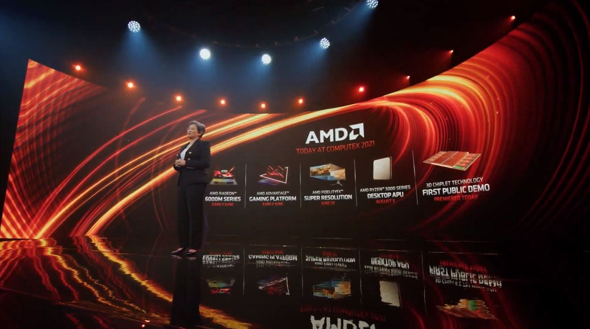
The AMD team surprised us here. What seemed like a very par-for-the-course Computex keynote turned into an incredible demonstration of what AMD is testing in the lab with TSMC’s new 3D Fabric technologies. We’ve covered 3D Fabric before, but AMD is putting it to good use by stacking up its processors with additional cache, enabling super-fast bandwidth, and better gaming performance. That’s the claim at any rate, and AMD showcased its new demo processor on stage at Computex. Here’s a deeper run-down into what it actually is.
3D Chiplets: The Next Step
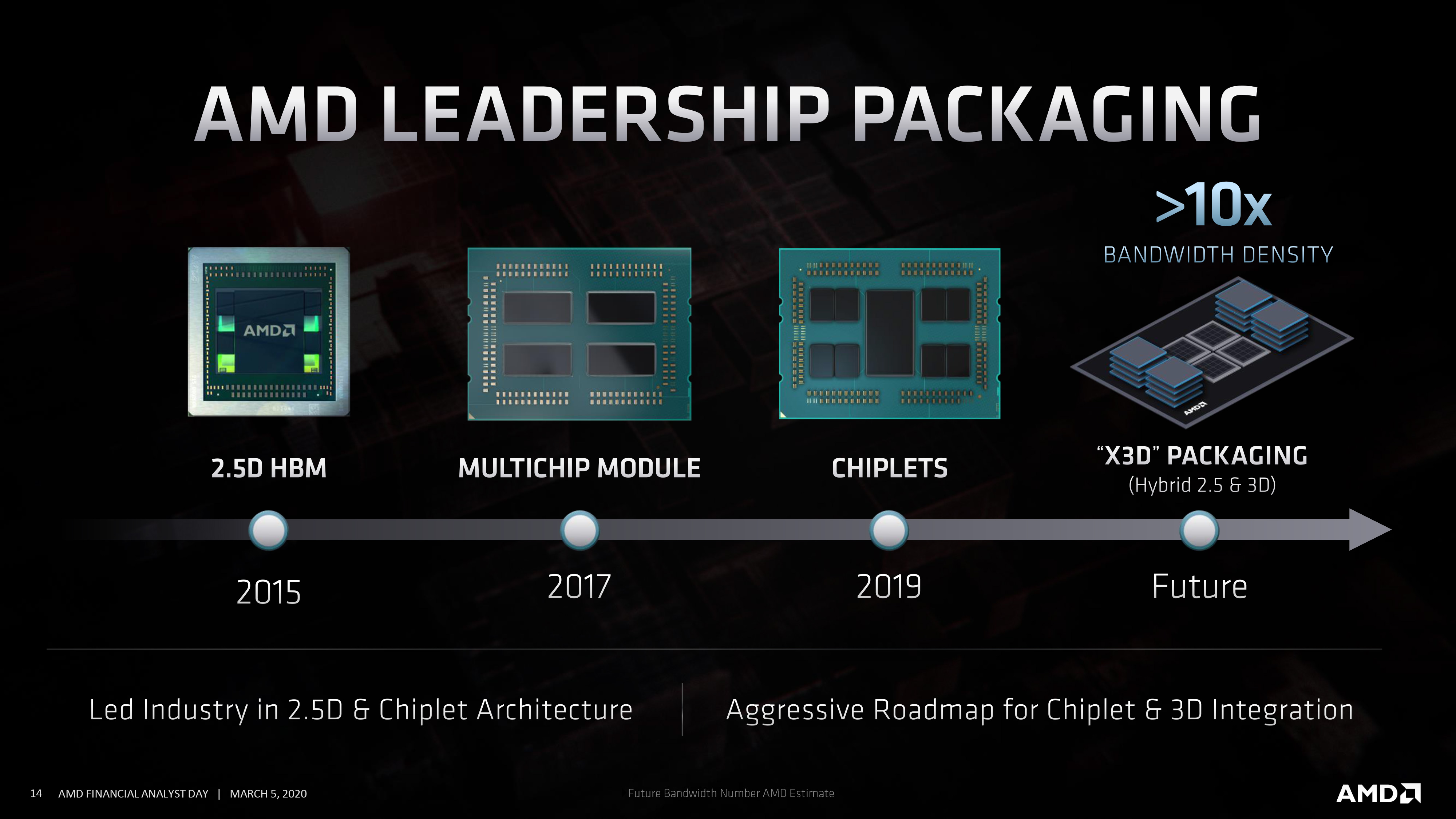
AMD announced it was looking into 3D stacking technologies with ‘X3D’ back in March 2020 at its Financial Analyst Day, with a very odd diagram showing a chiplet processor with what looked like stacks of HBM or some sort of memory around the outside. At the time AMD said it was a mix of 2.5D and 3D packaging technologies enabling 10x bandwidth density or higher. The ‘X’ in ‘X3D’ was meant to stand for Hybrid, and the technology was set for ‘the future’. Since then TSMC has announced its 3D Fabric line of technologies, a broad name for its combination of 2.5D and 3D integration offerings.
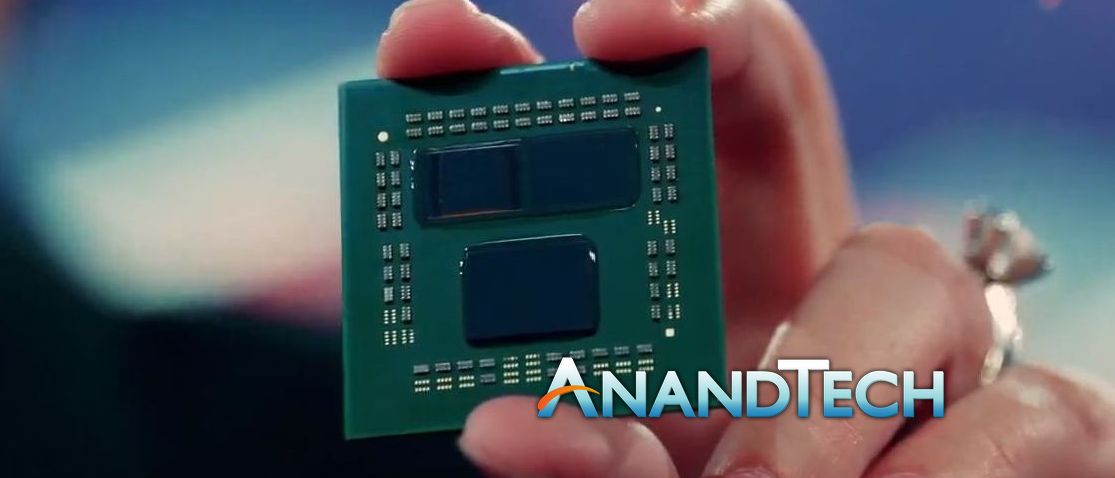
Today AMD presented the first stage of its 3D chiplet journey. The first application is a stacked cache on top of a standard processor chiplet. On stage, Lisa Su showcased one of AMD’s Ryzen 5000 dual-chiplet processors with Zen 3 cores. On one of the compute chiplets, a 64 MB SRAM built on TSMC’s 7nm was integrated on the top, effectively tripling the amount of cache that the cores have access to.
That means that the original Ryzen 5000 chiplet, with eight cores having access to 32 MB of L3 cache, now becomes an eight-core complex with access to 96 MB of L3 cache. The two dies are bonded with Through Silicon Vias (TSVs), passing power and data between the two. AMD claims that the total bandwidth of the L3 cache increases to beyond 2 TB/sec, which would technically be faster than the L1 cache on the die (but with higher latency).
As part of the chip diagram, the TSVs would be direct copper-to-copper bonding. The cache die is not the same size as the core complex, and as a result additional structural silicon is needed to ensure that there is equal pressure across both the bottom compute die and the top cache die. Both dies are thinned, with the goal to enable the new chiplet in the same substrate and heatspreader technology currently in use in Ryzen 5000 processors.
The prototype processor shown on stage had one of its chiplets using this new caching technology. The other chiplet was left as standard to show the difference, and the one chiplet that had the cache die ‘exposed’ made it obvious and comparable with the regular non- integrated chiplet. CEO Dr. Lisa Su said that the 64 MB SRAM in this case is a 6mm x 6mm design (36 mm2), which puts it at just under half the die area of a full Zen 3 chiplet.
In a full product Lisa explained that all the chiplets would have the stacked cache enabled, for 96 MB of cache per chiplet, or 192 MB total for a processor like this that has 12 or 16 cores.
As part of the technology, it was explained that this packaging enables a >200x interconnect density compared to regular 2D packaging (which is something we already know from HBM stacking), a >15x density increase compared to microbump technology (a shot straight across the bow of Intel’s Foveros), and >3x better interconnect efficiency compared to microbumps. The TSV interface is a direct die-to-die copper interconnect, meaning that AMD is using TSMC’s Chip-on-Wafer technology. Dr Su claimed on stage that these features make this the most advanced and flexible ‘active-on-active’ chip stacking technology in the industry.
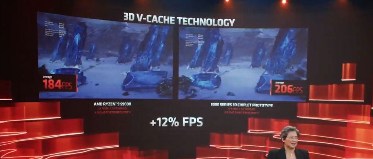
As for performance demonstrations, AMD compared a before and after using Gears of War 5. On one side was a standard Ryzen 9 5900X 12-core processor, while the other was a prototype using the new 3D V-Cache built upon a Ryzen 9 5900X. Both processors were fixed at 4 GHz, and paired with an un-named graphics card.
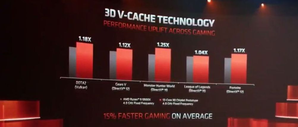
In this scenario the comparison point is that one processor has 64 MB of L3 cache, while the other has 192 MB of L3 cache. One of the selling points of Ryzen 5000 processors was the extended L3 cache available to each processor to help with gaming performance, and moving that up to 96 MB per chiplet extends that advantage even further, with AMD showing a +12% FPS gain (184 FPS vs 206 FPS) with the increased cache size at 1080p. Over a series of games, AMD claimed +15% average gaming performance:
DOTA2 (Vulkan): +18%
Gears 5 (DX12): +12%
Monster Hunter World (DX11): +25%
League of Legends (DX11): +4%
Fortnite (DX12): +17%
This is not an exhaustive list by any means, but it makes for interesting reading. AMD’s claim here is that a +15% bump is akin to a full architecture generation jump, effectively enabling a rare improvement through philosophical design differences. Here at AnandTech we would like to note that as it becomes harder to drill down into new process nodes, philosophical design enhancements might become the main driver of future performance.
AMD says that it has made great strides with the technology, and is set to put it into production with its highest-end processors by the end of the year. It wasn’t stated on what products it would be coming to, whether that was consumer or enterprise. Apropos of this, AMD has said that Zen 4 is set for launch in 2022.
The AnandTech Analysis
Well that was unexpected. We knew that AMD was going to be investing in TSMC’s 3D Fabric technology, but I guess we didn’t expect it to be this soon or with a demo on a desktop processor first.
Starting with the technology, this is clearly TSMC’s SoIC Chip-on-Wafer in action, albeit with only two layers. TSMC has demonstrated twelve layers, however those were non-active layers. The problem with stacking silicon is going to be in the activity, and subsequently thermals. We’ve seen with other TSV stacked hardware, like HBM, that SRAM/memory/cache is the perfect vehicle for this as it doesn’t add that much to the thermal requirements of the processor. The downside is that the cache you stack on top is little more than just cache.
This is where AMD and Intel’s stacking differs. By using TSVs rather than microbumps, AMD can get greater bandwidth and power efficiency out of TSVs, but also stack multiple chiplets high if needed. TSVs can carry power and data, but you still have to design around the two for cross signaling. Intel’s Foveros technology, while it is also 3D stacking, it relies on microbumps between the two chiplets. These are bigger and power-hungry, but allow Intel to put logic on both the lower die and upper die. The other element is thermals – usually you want the logic on the top die to manage the thermals better as it is close to the heatspreader/heatsink, but moving logic further away from the substrate means that power has to be transported up to the top die. Intel is hoping to mix microbumps and TSVs in upcoming technologies, and TSMC has a similar roadmap for the future for its customers.
Moving to the chiplet itself, it was claimed that the 64 MB L3 cache chiplet is 6mm x 6mm, or 36 mm2, and is built on TSMC 7nm. The fact that it is built on TSMC 7nm is going to be a critical point here – you might think that a cache chiplet might be better suited to a cheaper process node. The tradeoff in cost is power and die area (yield at such a small die size isn’t worth considering). If AMD is to make these cache chiplets on TSMC 7nm, then that means a Zen 3 with additional cache requires 80.7 mm2 for the Zen 3 chiplet as normal, then another 36 mm2 for the cache, effectively requiring 45% more silicon per processor. While we’re currently in a silicon shortage, this might have an effect on how many processors are made available for wider use. This might be why AMD said it was looking at ‘highest-end’ products first.
Now adding 64 MB of cache to a chip that already has 32 MB of L3 cache isn’t as straightforward as it seems. If AMD is directly integrating it as an adjacency to the L3 cache, then we have a dual-tiered L3 cache. Likely accessing that 64 MB requires more power, but that provides greater bandwidth. It would depend on the workload if the regular 32 MB is enough, compared to the extra 64 MB provided by the stacked die. We could see the extra 64 MB seen as an equivalent L4 cache, however the issue here is that in order for that extra 64 MB to go out to main memory, it has to pass through the main chiplet under it. That’s an additional power draw worth noting. I am very interested in seeing how the memory profile from the perspective of a core comes out with this extra chiplet, and how AMD is integrating that into the structure. AMD has stated that it is an SRAM-based design, so unfortunately it isn’t anything fancy like persistent memory, which would have been a whole different design ethos. By sticking to SRAM it means that at least it can seamlessly provide performance uplifts.
On the performance, we’ve seen L3 cache depth improve gaming performance, both for discrete and integrated gaming. However, increased L3 cache depth doesn’t do much else for performance. This was best exemplified in our review of Intel’s Broadwell processors, with 128 MB of L4 cache (~77 mm2 on Intel 22nm), wherein the extra cache only improved gaming and compression/decompression tests. It will be interesting to see how AMD markets the technology beyond gaming.
Finally, interception into the mainstream - AMD says that it is ready to start integrating the technology into its high-end portfolio with production at the end of the year. AMD has said that Zen 4 on 5nm launch is in 2022. Based on previous timescales, we have predicted that AMD’s next processor family is roughly a Feb 2022 launch. Whether that would be Zen 4 it’s unclear at this point, but also Zen 4 is on 5nm and AMD is showcasing this 3D V-Cache on 7nm. Whether AMD has plans to monetize this feature on 7nm, or whether it might combine a 5nm Zen 4 chiplet with a 7nm 64 MB cache chiplet is unclear. It wouldn’t be too difficult to combine the two, however I suspect that AMD might want to push its caching technology into more premium products than Ryzen desktop. We might see special one-off editions as the technology ramps through the stack.
To conclude, I have a number of questions I’d like to ask AMD. I’m hoping that I will get some answers, and if I do, I’ll cycle back with the details.
You may have heard of NVMe over Fabrics, or its acronym NVMe-oF, but you may still not be clear on what exactly it is and how it will impact or affect your IT infrastructure. Here’s NVMe-oF explained.
NVMe – What is it?
Before we dive into NVMe-oF let’s take a step back to make sure we understand the foundation – NVMe.
Early flash storage devices were connected via SATA or SAS – protocols that were developed decades ago for hard disk drives (HDDs) and are still widely used for data infrastructure. SATA and SAS connected flash storage provided huge performance gains over HDDs. Yet, as speeds increased – on CPUs, backplanes, DRAM, and networks – the SATA and SAS protocols began to limit the performance from flash devices. SATA and SAS protocols accounted for HDD characteristics, such as rotational delay, head seek times, etc. that add unnecessary complexity for flash-based media. In order to take full advantage of flash storage performance, the Non-Volatile-Memory-Express (NVMe) protocol was created (version 1.0 in early 2008).
As the name implies, NVMe was designed assuming flash memory, not disk, was the storage target. As a result, it was developed as a much more efficient (faster) protocol, and NVMe devices use the PCIe electrical interface to communicate with CPUs, DRAM, etc. With many more IO lanes than SAS or SATA, NVMe delivers extremely high performance. As my colleague, Erik Ottem said during a recent webinar, NVMe is a divided 12-lane highway versus the two-lane country road of the past (i.e. SAS and SATA). See the video below:
Today, NVMe is often used in servers to connect a flash drive to the PCIe bus as direct attached storage, giving the server a more efficient way to use flash media. However, the challenge with using NVMe in that way is the flash device is not accessible by any other systems beyond the server it is attached to – potentially creating a situation where it is underutilized when other servers could benefit from additional flash.
Enter Fabrics
The NVMe protocol is not limited to simply connecting flash drives, it may also be used as a networking protocol. When used in this context, a “fabric” enables any-to-any connections among elements. This is to distinguish it from a network, which may restrict the connections possible among the attached elements.
NVMe over Fabrics (NVMe-oF) are enabling organizations to create a very high performance storage network with latencies that rival direct attached storage (DAS). As a result, flash devices can be shared, when needed, among servers.
NVMe-oF – Fibre Channel vs. Ethernet
But, when it comes to networking, you may be wondering if this protocol is limited to fibre or ethernet? The good news is that it can run on both traditional fibre channel switches and IP switches. Most modern fibre channel switches already have updated firmware and are able to support the NVMe-oF protocol today. Ethernet, which is supported by several standards, offers additional choices for IT infrastructure.
Leveraging NVMe-oF with Fibre Channel (FC) should be straight forward for environments already invested in FC infrastructure. FC is designed for storage and can support both legacy SCSI traffic and NVMe traffic simultaneously. Since most organizations will integrate NVMe-oF into an existing data center, current support of both protocols enables them to make the conversion at a pace comfortable for them.
NVMe-oF via Ethernet typically counts on Remote Direct Memory Access (RDMA), which enables two computers on the same network to exchange memory contents without involving the processor. While RDMA is not specifically a storage protocol, it can be enabled in storage networking with protocols like RoCE (RDMA over Converged Ethernet), and iWARP (internet wide area RDMA protocol). A newcomer to the Ethernet NVMe-oF implementations is NVMe/TCP, which enables customers to run NVMe-oF over existing Ethernet infrastructure, taking advantage of legacy or non-RDMA infrastructure while possibly incurring a small performance penalty.
Deciding Between the NVMe-oF Options
Up until the release of NVMe/TCP, NVMe/FC had clear advantages for many enterprises. It was able to run both SCSI and NVMe at the same time, and it also had an auto-discovery capability that made adding new servers or storage to the fabric easier. The challenge for FC is outside of the enterprise, it isn’t as popular as Ethernet-based use cases, like NFS and iSCSI. RoCE and iWARP are emerging in more implementations, and vendors providing these solutions claimed some performance advantages over FC because of RDMA’s direct memory access capabilities. NVMe/TCP, although late to the game, does have some advantages and seems to be a good match for organizations without a legacy FC infrastructure and not requiring RDMA.
NVMe-oF: Need and Timing
When IT planners aggressively switch to NVMe-oF is largely a function of need and timing. The first step to NVMe for most organizations is an NVMe Flash Array with traditional networking connections to the storage network. While these systems generate IOPS approaching the millions, the reality is that there are very few workloads that require more than the performance of these systems.
However, there is an emerging class of workloads that can take advantage of all the performance and low latency of an end-to-end NVMe system.
Additionally, a NVMe-oF storage target can be dynamically shared among workloads – providing an “on-demand” or composable storage resource that provides additional benefits, including flexibility, agility, and greater resource efficiency.
Customers who operate workloads that demand high performance and low latency should evaluate the advantages and disadvantages of shifting to an end-to-end NVMe-oF implementation. However, IT planners must be very careful in selecting all infrastructure elements (servers, networking, etc.) used to eliminate any performance bottlenecks due to existing IT equipment.
Next Steps
If you want to learn more, join me in an upcoming webinar on NVMe-oF. I will cover everything you need to know about NVMe-oF, how it can transform your business, and what the next steps are when evaluating this technology.
Watch the video at the end of this article to see more examples!
You've all seen these kinds of pictures where a person's face is "toonified" into an anime character.
Many of you must have seen other kinds of image transformations like this, where an image is changed to follow the style of a certain artist.
Style Transfer example
Here, an even more challenging task could be something like this, where an image is transformed into another season or time of the day.
Results from the paper. (top) Summer to winter translation and (bottom) day to night translation. Liang et al., 2021
What you have not seen yet is the time it takes to produce these results and the actual resolutions of the produced pictures. This new paper is completely transparent towards this as it attacks exactly this problem. Indeed, compared to most approaches, they translate high-definition 4K images, and this is done in real-time. In this work, they showed their results on season translation, night and day translations, and photo retouching, which you've been looking at just above. This task is also known as 'image-to-image translation', and all the results you see here were produced in 4K. Of course, the images here were taken from their paper, so it might not look that high-quality here. Please look at their paper or try their code if you are not convinced!
These are the most amazing results of this paper:
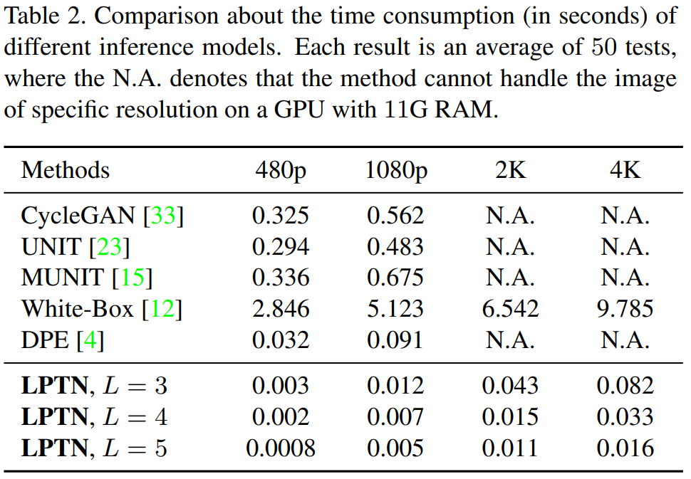
Here, you can see their technique below called LPTN, which stands for Laplacian Pyramid Translation Network. Look at how much less time it took LPTN to produce the image translations where most approaches cannot even do it as this amount of definition is just too computationally demanding. And yes, this is in seconds. They could translate 4K images in not even a tenth of a second using a single regular GPU. It is faster than all these approaches on 480p image translations! And yes, it is not eight times faster, but 80 times faster on average! But how is that possible? How can they be so much more efficient and still produce amazing and high-quality results?
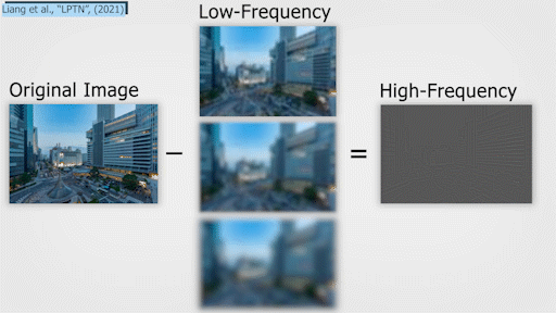
This is achieved by optimizing the fact that illumination and color manipulation, which relates to the style of an image, is contained in the low-frequency component of an image.
Low-Frequency vs. High-Frequency images
Whereas the content details, which we want to keep when translating an image into another style, can be adaptively refined on high-frequency components. This is where it becomes interesting. These two components can be divided into two tasks that can be performed simultaneously by the GPU. Indeed, they split the image into low-resolution and high-resolution components, use a network to process the information of the low-frequency or the style of the image, and render a final image merging this processed style with the refined high-frequency component, which is the details of the image but adapted by a smaller sub-network to fit the new style. Thus dodging the unavoidable heavy computation consumption when processing the high-resolution components in the whole network. This has been a long-standing studied field achieved with a popular technique called Laplacian Pyramid. The main idea of this Laplacian Pyramid method is to decompose the image into high and low-frequency segments and reconstruct it afterward.
First, we produce an average of the initial image, making it blurry and removing high-frequency components.
Averaging process.
This is done using a kernel that passes through the whole image to round batches of pixels together. For example, if they take a 3 by 3 kernel, it would go through the whole image averaging 3 by 3 patches removing all unique values. They are basically blurring the image by softening the edges.
Low-Frequency vs. High-Frequency images
Then, the difference between this blurry image and the initial image is saved to use at the end of the algorithm to re-introduce the details, which are the high-frequency components. This is repeated three times with bigger and bigger averaging kernels producing smaller and smaller low-frequency versions of the image having less and less high-frequency details.
If you remember, these low-frequency versions of the image contain information about the colors in the image and illumination. Indeed, they are basically just a blurred low-quality version of our image, which is why the model is so much more efficient. This is convenient since they are smaller versions of the image, and this is the exact information we are trying to change when translating the image into another style.
Input image transformation steps.
Meaning that using these low-frequency versions is much more computationally efficient than using the whole image directly, but they are also focused on the information we want to change in the image, which is why the results are so great.
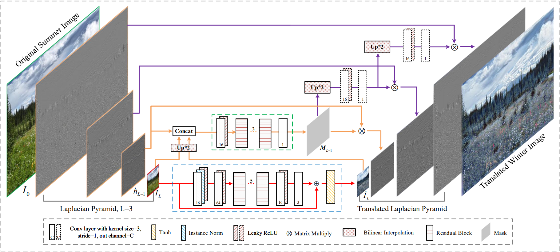
Full LPTN network. Liang et al., 2021
This lower-quality version of the image can be easily translated using an encoder-decoder, just like any other image translation technique we previously mentioned, but since it is done on a much lower quality image and a much smaller image, it is exponentially faster to process. The best thing is that the quality of the results only depends on the initially saved high-frequency versions of the image sent as input which is not processed throughout the whole network. This high-frequency information is simply merged at the end of the processing with the low-frequency image to improve the details. Basically, it is so much faster because the researchers split the image's information in two: low-frequency general information and detailed high-frequency information. Then, they send only the computational-friendly part of the image, which is exactly what we want to transform, the blurry, low-quality general style of the image, or in other words: the low-frequency information. Then, only fast and straightforward transformations are done on the high-frequency parts of the image to resize them and merge them with the blurry newly-stylized image, improving the results by adding details on all edges in the picture.
And voilà! You have your results with a fraction of the time and computational power needed. This is brilliant, and the code is publicly available if you would like to try it, which is always cool!
Thank you for reading!
Watch the video
Come chat with us in our Discord community:Learn AI Together and share your projects, papers, best courses, find Kaggle teammates, and much more!
If you like my work and want to stay up-to-date with AI, you should definitely follow me on my other social media accounts (LinkedIn, Twitter) and subscribe to my weekly AI newsletter!
To support me:
The best way to support me is by being a member of this website or subscribe to my channel on YouTube if you like the video format.