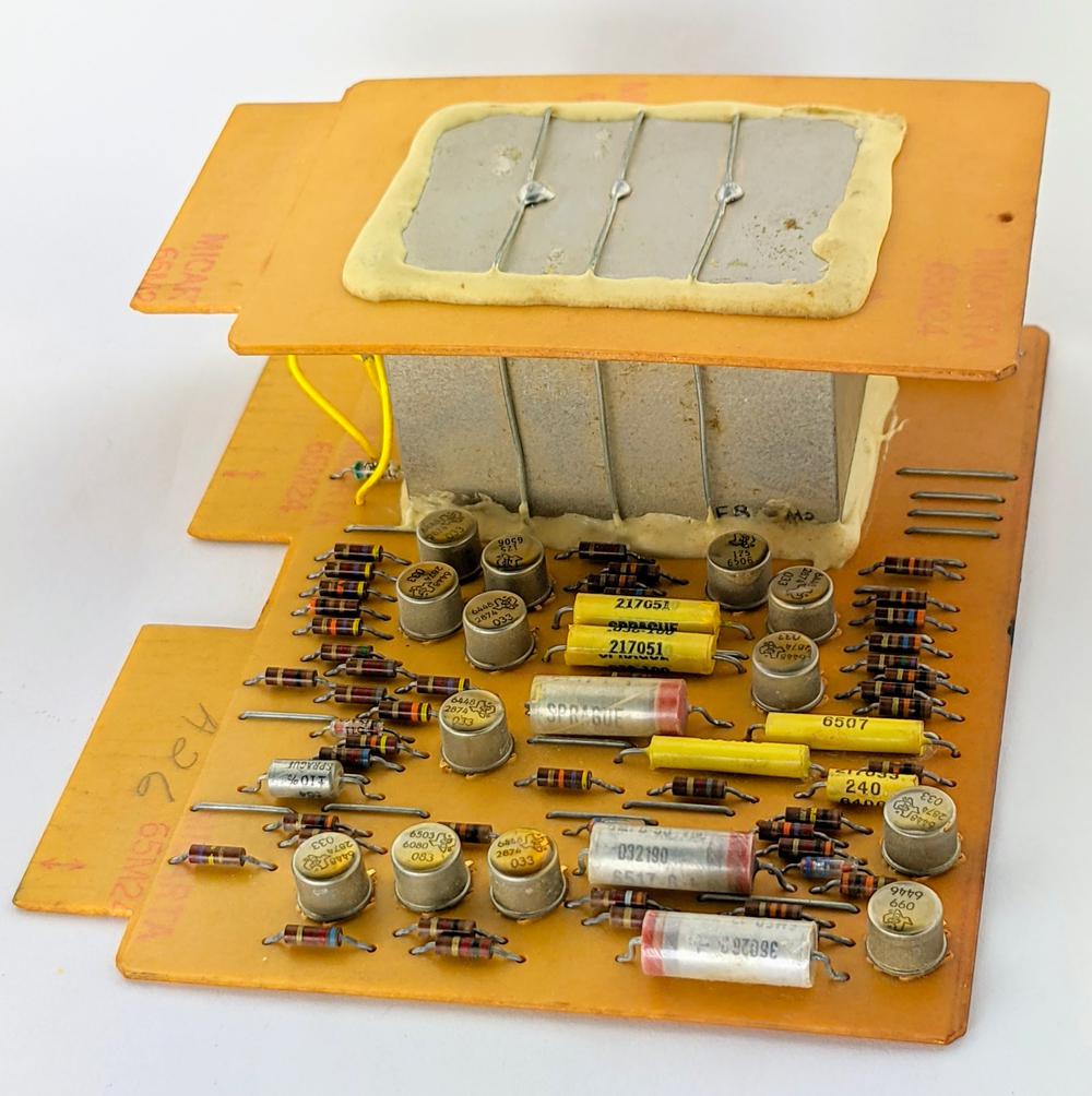
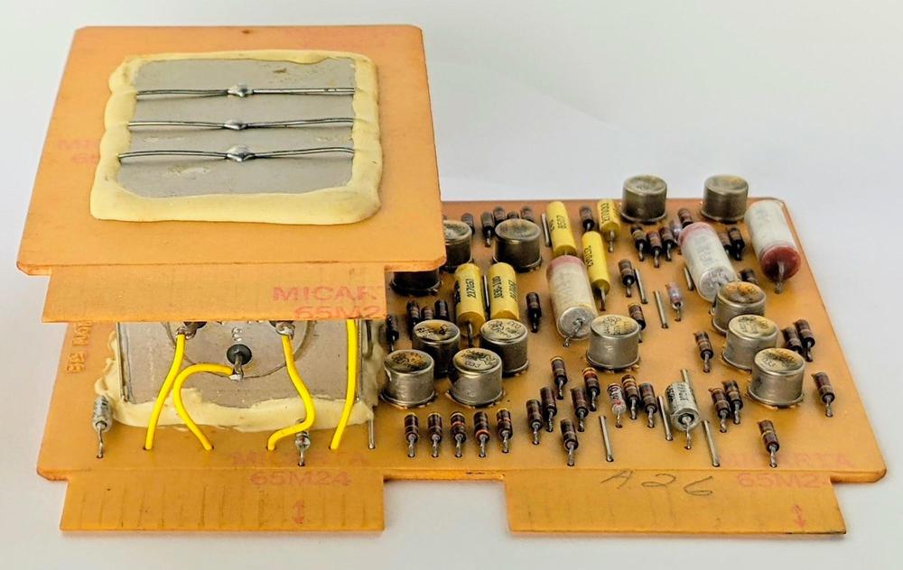
The vintage IBM circuit board below has a large metal block on it that caught my attention, so I investigated it in detail. It turns out that the board is part of a modem, and the large metal box is a transformer. This blog post summarizes what I learned about this board, along with a bit of history on modems.
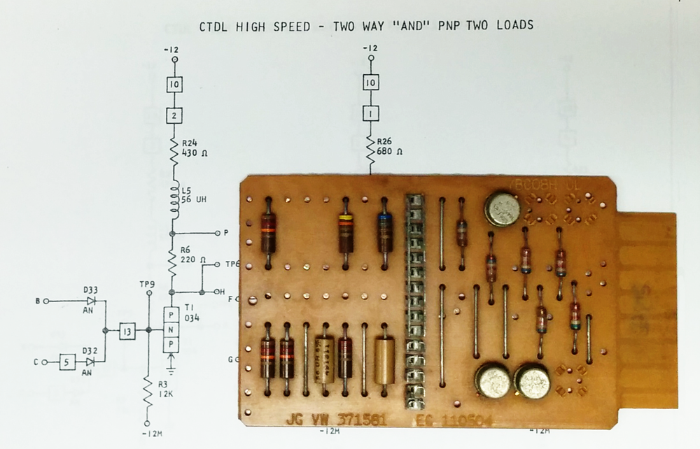
This board is a Standardized Modular System (SMS) card, but a very unusual one. In the late 1950s, IBM introduced the Standardized Modular System card, small circuit boards that held a simple circuit, and used these boards to build computers and peripherals into the mid-1960s. The idea was to design a small number of standardized boards that implemented logic functions and other basic circuits. The number of different board designs spiraled out of control, however, with thousands of different types of SMS cards. (I've made an SMS card database describing over 1400 different cards.)
This is a typical SMS card, implementing a triple AND gate.
Most SMS cards look like the one above, so the card with the metal block struck me as very unusual. Although some SMS cards are double-width "twin cards", I'd never seen one with a large metal block sandwiched between two boards, so it got my curiosity.
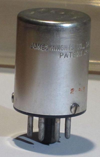
One suggestion was that the metal box was a temperature-compensated crystal oven (TCXO). A TCXO is often used when a high-precision frequency source is required. The frequency of a quartz crystal varies with temperature, so by putting the crystal in a temperature-controlled module (like the one below), the frequency remains stable.
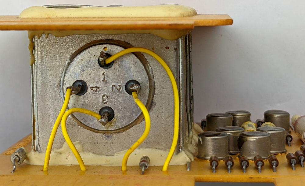
However, measurements of the module by Curious Marc and Eric Schlaepfer (TubeTimeUS) determined that the metal box was a large transformer (1:1 ratio, about 8 mH inductance). The photo below shows the four connections to the windings, while the external metal wires grounded the case. The transformer is heavy—the board weighs almost exactly one pound—so it's probably filled with oil.
The transformer on the modem board.
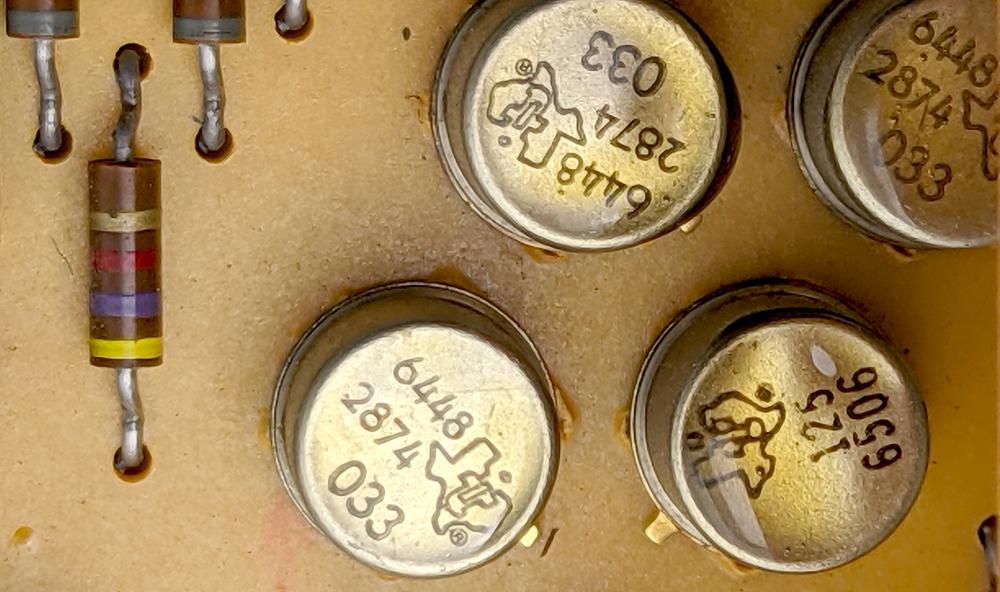
The board shows its age through its germanium transistors, which were used before silicon transistors became popular. Most of the transistors are PNP, apparently because it was easier to produce PNP germanium transistors than NPN. (Silicon transistors are the opposite with NPN transistors much more common than PNP, largely because the electrons in NPN transistors move more easily than the holes in PNP transistors, giving better performance to NPN transistors.)
Closeup of the Texas Instruments transistors. Most of the transistors on the board were PNP type 033.
I found a document1 that gave the board's part number as a transmitter board for an IBM modem, transmitting data across phone lines. The large transformer would have been used to connect the modem to the phone lines while maintaining the necessary isolation. The modem used frequency-shift keying (FSK), using one frequency for a 1 bit and a second frequency for a 0 bit. I reverse-engineered the board by closely studying it, and discovered that the board generates these two frequencies, controlled by a data input line. This confirmed that the board was a modem transmitter board.
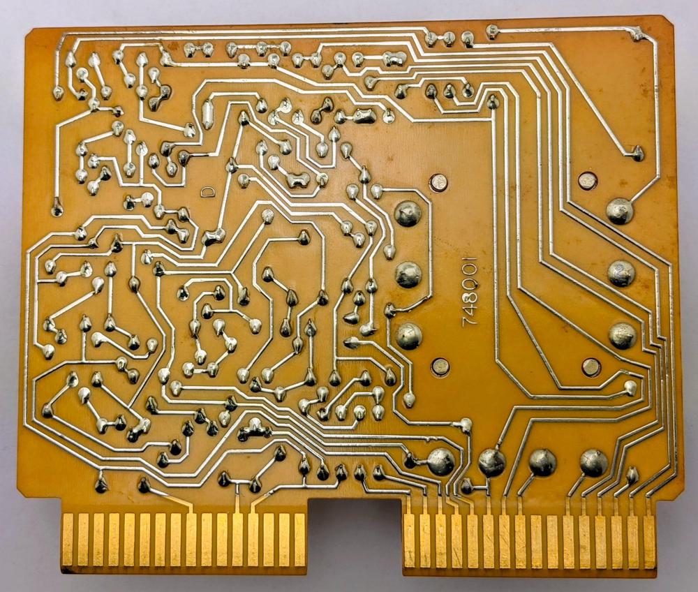
The photo below shows the underside of the board, with the traces that connect the components. The board is single-sided, with traces only on the underside, so traces tend to wander around a lot, using jumper wires on the other side to cross over other traces. (It took me a while to realize that the transformer's case was just wired to ground, since the trace wanders all over the board before reaching the ground connection.) At the bottom of the board are the two gold-plated 16-pin connectors that plug into the system's backplane. The connector on the left provides power, while the connector on the right has the signals.
The underside of the printed circuit board for the modem card.
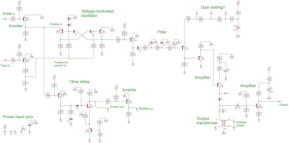
The result of my reverse-engineering is the schematic below. (Click for a larger version.) The circuit seems complicated for a board that just generates a varying frequency, but it took a lot of parts to do anything back then. At the left of the schematic are the board's two inputs: a binary data signal, and an enable signal that turns the oscillator on. Next are the oscillator that produces the signal, and a 13 millisecond delay (both discussed below). The output from the oscillator goes through a filter that makes it somewhat more sine-like. The signal is then amplified to drive the transformer, as well as to produce a direct output.
Reverse-engineered schematic of the IBM modem board. (Click this image, or any other, for a larger version.)
The oscillator
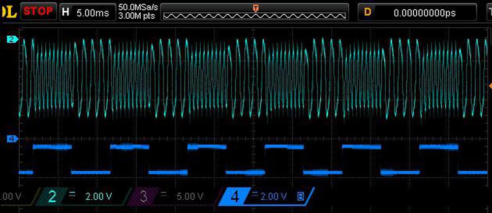
The oscilloscope trace below shows the output that I measured from the board after powering it up. The blue line shows the data input, while the cyan waveform above shows the frequency output. You can see that the output frequency is different for a "1" input and a "0" input, encoding the data. (The height also changes, but I think that's just a side-effect of the circuit.)
Oscilloscope trace showing how the frequency of the output signal varies with the input data.
The modem is supposed to generate frequencies of 1020 Hertz for a "mark" (1) and 2200 Hertz for a "space" (0). However, I measured frequencies of 893 and 1920, about 13% too low. This seems like reasonable accuracy for components that are 55 years old. (I don't know what the expected accuracy was at the time. There aren't any adjustments, so the frequencies probably weren't critical. Also, since the two frequencies differ by more than a factor of two, there's a large margin.)
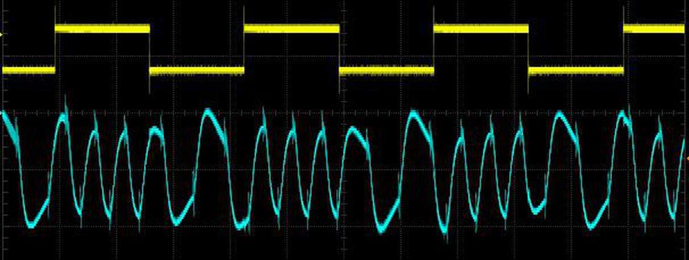
The modem operated at up to 600 baud. This corresponded to 100 characters per second for 6-bit characters, or 75 characters per second for 8-bit characters. The oscilloscope trace below shows the signal changing at 600 baud. At this rate, one bit is represented by only 1.7 cycles of the slower frequency, so the receiver doesn't have a lot of information to distinguish a 0 or a 1 bit. Also note that the waveform is somewhat distorted, not a clean sine wave.
The output signal when fed bits at 600 baud (i.e. a 300 Hertz square wave).
The heart of this board is the frequency-shift keying oscillator that generates the variable output frequency.2 The input data bit selects one of two control voltages to the oscillator, controlling its output frequency.
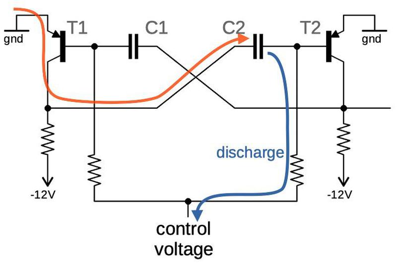
The oscillator is a fairly common transistor-pair circuit. The diagram below illustrates how it works. (It uses PNP transistors and runs on -12 volts, so ground is the higher voltage, which may be a bit confusing.) Suppose transistor T1 is on and T2 is off. Capacitor C2 will discharge through resistor R2, as shown. When its voltage reaches about -0.6 volts, T2 will turn on. This will pull the right side of C1 up to ground; it was previously at -12 volts because of R4. This causes the left side of C1 to jump up to about +12 volts, turning off T1.
The process then repeats on the other side, with C1 discharging through R1 until T1 turns off and T2 turns on. The result is that the circuit oscillates. The discharge rate is controlled by the values of R1 and R2, and the control voltage; a lower voltage will cause the capacitors to discharge faster and thus faster oscillations.
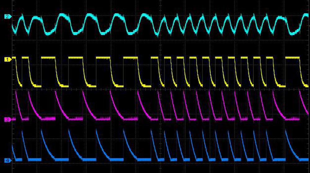
Oscilloscope traces of the oscillator, showing the alternating decay cycles.
The traces above show the action of the oscillator, producing the cyan output signal. The yellow curve shows the voltage on the left side of C2, the pink trace shows the voltage on the left side of C1, and the blue trace shows the voltage on the right side of C2. The pink and blue traces show the alternating discharge cycles for the capacitors; the faster discharge yields a higher output frequency.
Schematic of the oscillator at the heart of the board.
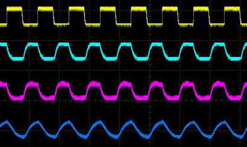
The output of the oscillator is essentially a square wave, so it goes through some resistor-capacitor filtering stages that shape it to better approximate a sine wave. The top line (yellow) shows the output of the oscillator, and the lines below show the signal as it progresses through the filter. The result is still fairly distorted, but much smoother than the original square wave.
The square wave signal and the results after filtering.
Delay circuit
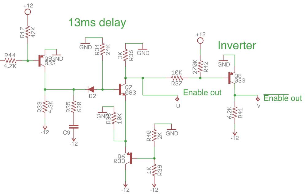
Another interesting circuit takes the enable signal and outputs this signal delayed by 13 milliseconds. When I reverse-engineered this circuit (below), I figured it was just buffering the signal but it appeared overly complex for that. I measured its behavior and discovered that it implements a delay.
Reverse-engineered schematic showing the 13ms delay circuit on the modem board.
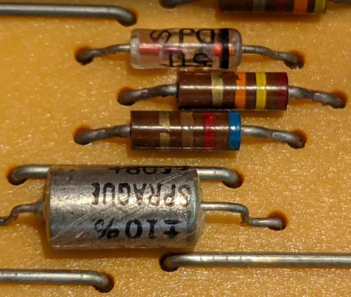
The circuit contains several buffers, but the heart of it is a resistor-capacitor delay. When the enable line is activated, the capacitor is pulled to -12V slowly through the resistors, creating the delay. The photo below shows the delay capacitor and associated resistors.
The diode (striped glass cylinder), resistors (brown striped components), and capacitor (larger metal cylinder) create the delay.
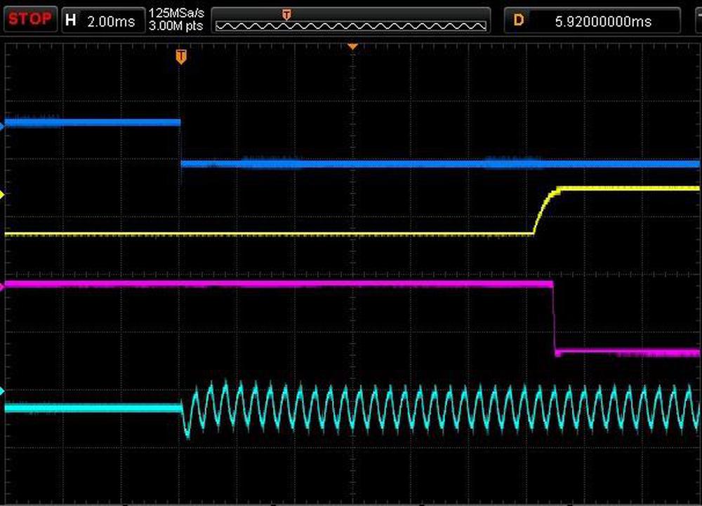
The oscilloscope trace shows the operation of the delay circuit. When the (inverted) enable line (blue) goes low, the signal output (cyan) immediately turns on. However, the enable outputs (yellow and pink) are delayed by about 13 milliseconds.
Oscilloscope trace of the delay circuit.
I don't know the reason behind this delay circuit. Maybe it gives the oscillator time to settle after being enabled? Maybe the modem protocol uses 13 milliseconds of signal to indicate the start of a new message?
Some background on Teleprocessing
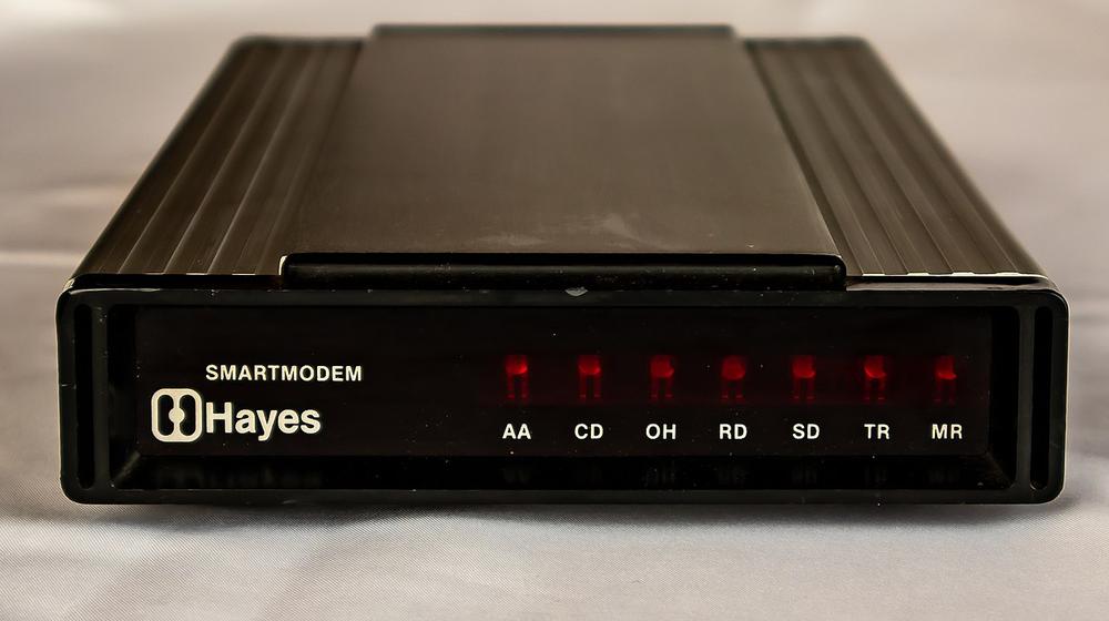
If you used computers in the 1990s, you probably used a dial-up modem like the one below to call a provider such as AOL through your phone line. The name "modem" is short for MOdulator-DEModulator, since it modulates the analog signal to encode the digital bits, as well as demodulating the received signal back to digital. In this way, the modem provided the connection between your computer's digital signals and the analog frequencies transmitted by phone lines.
The history of modems goes back much further, though. IBM introduced what they called "Teleprocessing" in the early 1940s, converting punch-card data to paper tape and sending it over telegraph lines for the U.S. Army.1 In the early 1950s, a device called Data Transceiver removed the intermediate paper tape, connecting directly to a telephone line. With the introduction of the IBM System/360 mainframe in 1964, Teleprocessing became widespread, used for many applications such as remote data entry and remote queries. Banking and airline reservations made heavy use of Teleprocessing. Timesharing systems allowed users to access a mainframe computer over remote terminals, kind of like cloud computing. Even the Olympics used Teleprocessing, transmitting data between widely-separated sites and a central computer that computed scores.
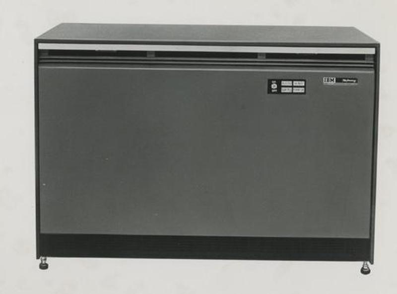
Back then, modems were large cabinets. The board that I examined could be used in an IBM 1026 Transmission Control Unit (below).3 This low cost unit was designed to "make a modest start toward satisfying your data communication requirements ... until it is time to step up to more powerful transmission control units". It could connect a computer such as the IBM 1401 to a single communications line.
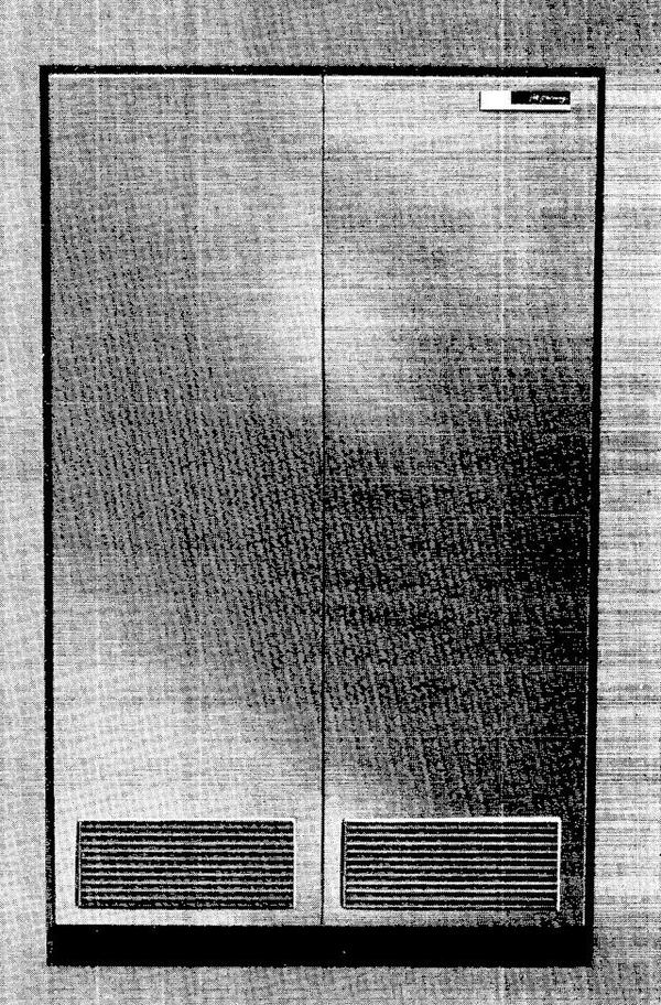
Larger installations could use the IBM 1448 Transmission Control Unit (below). This refrigerator-sized cabinet was 5 feet high and could support up to 40 communications links.
Nowadays, people often use a cable modem or DSL modem to connect to the Internet. Fortunately technology has greatly improved and these modems aren't the large cabinets of the 1960s. Speeds have also greatly improved; a modern 180 Mbps network connection is 300,000 times faster than the 600 baud modem board that I examined. At that rate, a web page that now loads in a second would have taken almost 3 months!
Conclusion
This may seem like an overly detailed analysis of a random circuit board. But I was curious about the board due to its unusual transformer. I also figured it would be interesting to reverse-engineer the board to see how IBM built analog circuits back in the 1960s. Hopefully you've enjoyed this look at a vintage modem board.
Side view of the modem SMS card. The transformer is the metal box at the left.
I announce my latest blog posts on Twitter, so follow me at kenshirriff. I also have an RSS feed. Thanks to Nick Bletsch for sending me the board. I discussed this board on a couple of Twitter threads and got a bunch of interesting comments.
Notes and references
from Hacker News https://ift.tt/2YcNcOQ
No comments:
Post a Comment
Note: Only a member of this blog may post a comment.