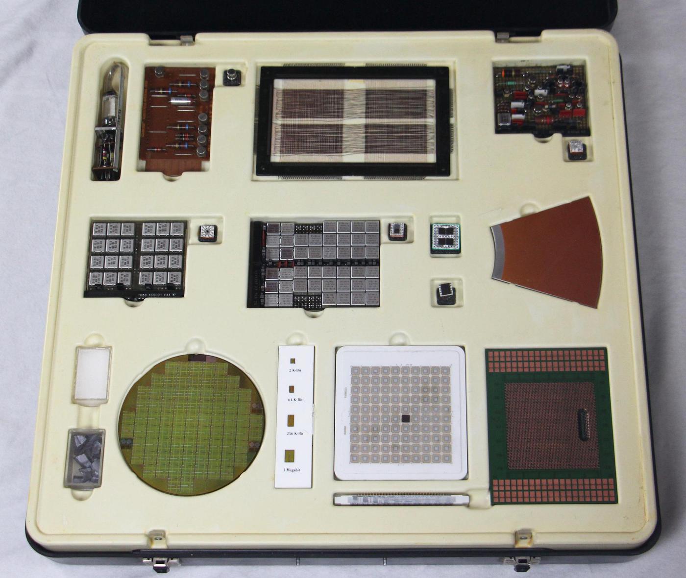
I recently received a vintage display box used by IBM to illustrate the progress of computer technology. This display case, created by IBM Germany1 in 1986 included technologies ranging from vacuum tubes and magnetic core memory to IBM's latest (at the time) memory chips and processor modules. In this blog post, I describe these items in detail and how they fit into IBM's history.
An IBM display box, showing components and board from different generations of computing. Click this (or any other photo) for a larger image.
First-generation computing: tube module
IBM is older than you might expect. It was founded (under the name CTR) in 1911 and produced punched card equipment for data processing, among other things. By the 1930s, IBM was producing complex electromechanical accounting machines for data processing, controlled by plugboards and relays.
The so-called first generation of electronic computers started around 1946 with the use of vacuum tubes, which were orders of magnitude faster than electromechanical systems. Appropriately, the first artifact in the box is an IBM pluggable tube module. The pluggable module combined a vacuum tube along with its associated resistors and capacitors. These modules could be tested before being assembled into the system, and also replaced in the field by service engineers. Pluggable modules were also innovative because they packed the electronics efficiently into three-dimensional space, compared to mounting tubes on a flat chassis.
Tube module from an IBM 604 Electronic Calculating Punch.
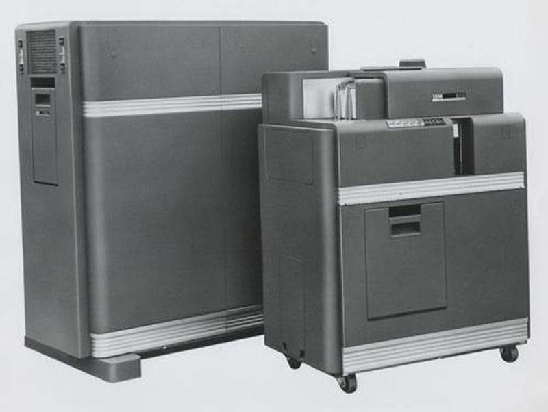
The pluggable tube module is from an IBM 604 Electronic Calculating Punch (1948). This large machine was not quite a computer, but it could add, subtract, multiply, and divide. It read 100 punch cards per minute, performed operations, and then punched the results onto new punch cards. It was programmed through a plugboard and could perform up to 60 operations per card. The IBM 604 was a popular product, with over 5600 produced. A typical application was payroll, where the 604 could compute various tax rates through multiplication.
The IBM 604 Electronic Calculating Punch behind a Type 521 Card Reader/Punch. Photo from IBM.
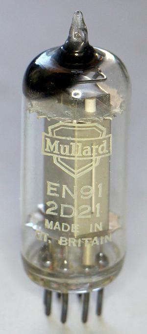
The 604 used many different types of tube modules. A typical module implemented an inverter, which could be used in an OR or AND gate.2 The tube module in the display box, however, is a thyratron driver, type MS-7A. The thyratron tube isn't exactly a vacuum tube since it is filled with xenon. This tube acts as a high-current switch; when activated, the xenon ionizes and passes the current. In the 604, thyratron tubes were used to drive relay coils or magnet coils in the card punch.3
A thyratron tube, type 2D21. This tube is from the pluggable module in the box.
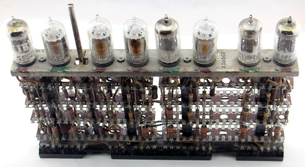
Although the 604 wasn't quite a computer, IBM went on to build various vacuum-tube computers in the 1950s. These machines used larger pluggable tube modules that each held 8 tubes.4 The box didn't include one of these modules—probably due to their size—but I've included a photo below because of their historical importance.
Second generation: transistors and SMS (Standard Modular System) card
With the development of transistors in the 1950s, computers moved into the second generation, replacing vacuum tubes with smaller and more reliable transistors. IBM based its transistorized computers on pluggable cards called Standard Modular System (SMS) cards. These cards were the building block of IBM's transistorized computers including the compact IBM 1401 (1959), and the larger 7000-series mainframe systems. A computer used thousands of SMS cards, manufactured in large numbers by automated machines.
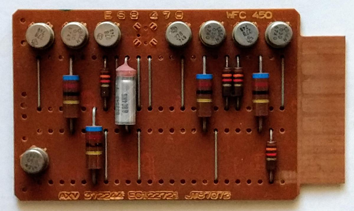
The photo below shows the SMS card from the box.5 The card is a printed circuit board, about the size of a playing card, with components and jumpers on one side and wiring on the back. A typical SMS card had a few transistors and implemented a simple function such as a gate. The cards used germanium transistors in metal cans as silicon transistors weren't yet popular. I've written about SMS cards before if you want more details.
The SMS card in the technology box, type AXV.
Third generation: SLT (Solid Logic Technology)
In 1964, IBM introduced the System/360 line of mainframe computers. The revolutionary idea behind System/360 was to use a single architecture for the full circle (360°) of applications: from business to scientific computing, and from low-end to high-end systems. (Prior to System/360, different models of computers had completely different architectures and instruction sets, so each system required its own software.) The System/360 line was highly successful and cemented IBM's leadership in mainframe computers for many years.
Although other manufacturers used integrated circuits for their third generation computers, IBM used modules called SLT (Solid Logic Technology), which were not quite integrated circuits. Each thumbnail-sized SLT module contained a few discrete transistors, diodes, and resistors on a square ceramic substrate. An SLT module was capped with a square metal case, giving it a distinct appearance. Although an SLT module doesn't achieve the integration of an IC, it provides a density improvement over individual components. Each small SLT module was roughly equivalent to a complete SMS card, but much more reliable.7 By 1966, IBM was producing over 100 million SLT modules per year at a cost of 40 cents per module.6
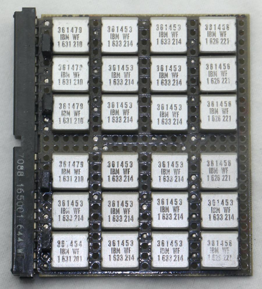
The board below is a logic board using 24 SLT modules. These modules implement AND-OR-INVERT logic gates, the primary logic circuit used in System/360. This board was probably part of the CPU.
A logic board using SLT modules. (The display box labeled this as an MST board though.)
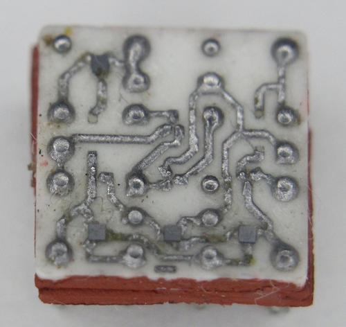
The photo below shows the circuitry inside an SLT module. This module has four transistors (the tiny gray squares). SLT modules typically include thick-film resistors, but none are visible in this module.
Closeup of an SLT module showing the tiny silicon dies mounted on the ceramic substrate.
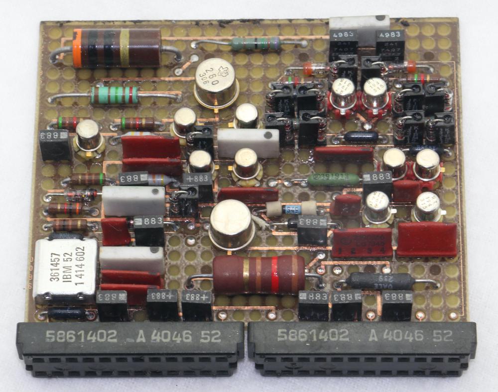
The box also has an SLT card with analog circuitry (maybe for the computer's core memory or power supply). This card has one SLT module, a simple module that contains four transistors (number 361457). I don't know why this board has so many discrete transistors; perhaps they are higher-power transistors than SLT modules provided.
A card using an SLT module (the metal square in the lower left).
Integrated circuits: MST (Monolithic System Technology)
For a few years, IBM used SLT modules while other computer manufacturers used integrated circuits. Eventually, though, IBM moved to integrated circuits, which they called Monolithic System Technology (MST). An MST module looks like an SLT module from the outside, but inside it contains a monolithic die (i.e. an integrated circuit) rather than the discrete components of SLT. MST was first used in 1969 for the low-end System/3 computer.
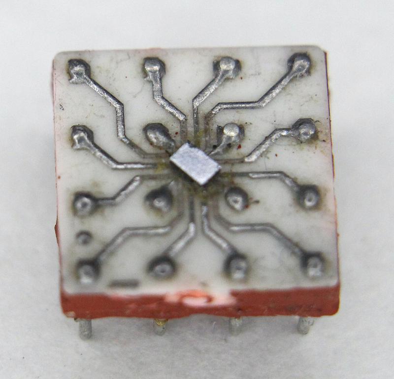
An MST module looks like an SLT module from the outside, but has an integrated circuit die inside.
The photo above shows the box's MST module. The silicon die is the tiny shiny rectangle in the middle, connected to the 16 pins of the module. The chip was mounted upside down, soldered directly to the substrate. This upside-down mounting is unusual; most other manufacturers used ceramic or plastic packages for integrated circuits, with the silicon die connected to the pins via bond wires.
Core memory
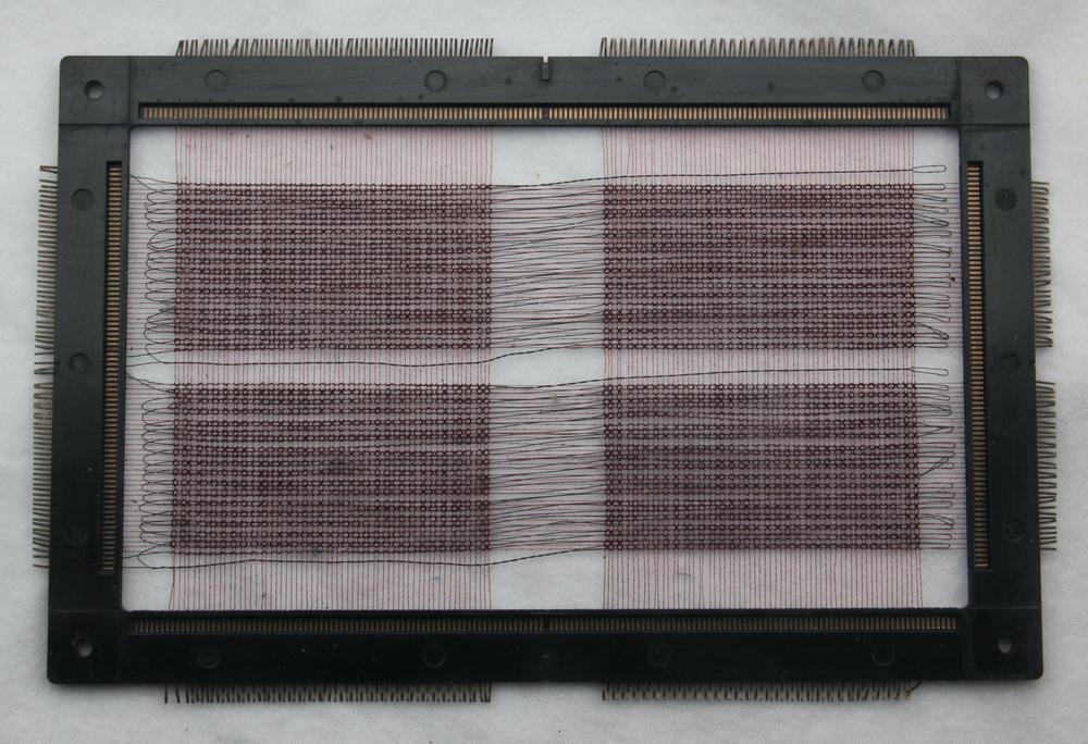
The box contains a core memory plane; most computers from the 1950s until the early 1970s used magnetic core memory for their main memory.8 This plane holds 8704 bits and is from a System/360 Model 20, the lowest-cost and most popular computer in the System/360 line.9
Core plane from a System/360 Model 20.
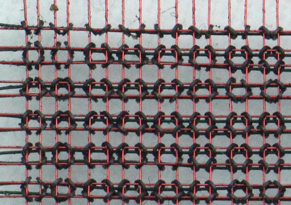
In core memory, each bit is stored in a tiny magnetized ferrite ring. The ferrite rings are organized into a matrix; by energizing a pair of wires, one bit is selected for reading or writing. Multiple core planes were stacked together to store words of data. Because each bit required a separate ferrite ring, magnetic core memory was limited in scalability. This opened the door for alternative storage approaches.
Closeup of the core plane, showing the wires through the tiny ferrite cores.
Semiconductor memory
IBM was an innovator in semiconductor memory and this is reflected in the numerous artifacts in the box that show off memory technology.10 Modern computers use a type of memory chip called DRAM (dynamic RAM), storing each bit in a tiny capacitor. DRAM was invented at IBM in 1966 and IBM continued to make important innovations in semiconductor memory.
Although magnetic core memory was the dominant RAM storage technique in the 1960s, IBM decided in 1968 to focus on semiconductor memory instead of magnetic core. The first computer to use semiconductor chips for its main memory12 was the IBM System/370 Model 145 mainframe (1970). Each chip in that computer held just 128 bits, so a computer might need tens of thousands of these chips.11 Fortunately, memory density rapidly increased, as shown by the dies below. I'll discuss the 2-kilobit chip in detail; my die photos of the others are in the footnotes13.
The box includes a display with four memory dies: 2 K-Bit, 64 K-Bit, 256 K-Bit, 1 Megabit.
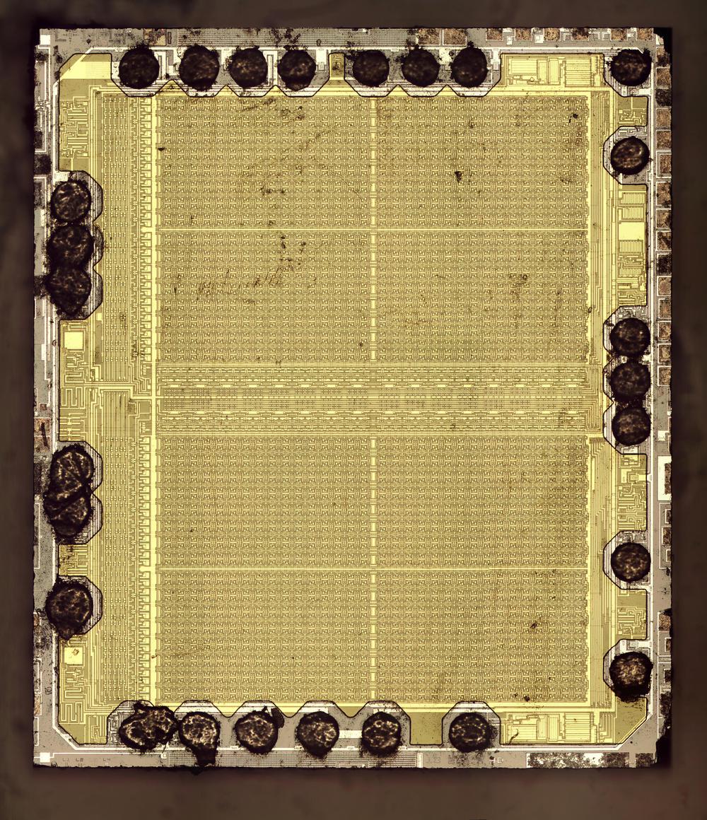
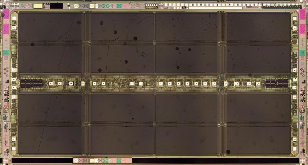
The photo below shows the 2-kilobit die14 under a microscope. It is a static RAM chip from 1973, not as dense as DRAM since it uses six transistors per bit. The tiny white lines on the chip are the metal layer on top of the silicon, wiring the circuitry together. Around the outside of the die are 26 solder bumps for attaching the chip to the substrate. Note that this chip is mounted upside down ("flip-chip") on the substrate, unlike most integrated circuits that use bond wires. The chip is covered with a protective yellowish film, except where the solder bumps are located.
Die photo of the 2-kilobit chip.
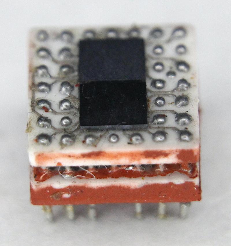
To increase the density of storage, four of these chips were mounted in a two-layer MST module, yielding an 8-kilobit module. The module in the box (below) has the square metal case removed, showing the silicon dies inside. These memory modules provided the main memory for the IBM System/370 models 115 and 125, as well as the memory expansion for the models 158 and 168 (1972).
The memory module has chips on two levels. This is an 8-kilobit module composed of four 2-kilobit chips.
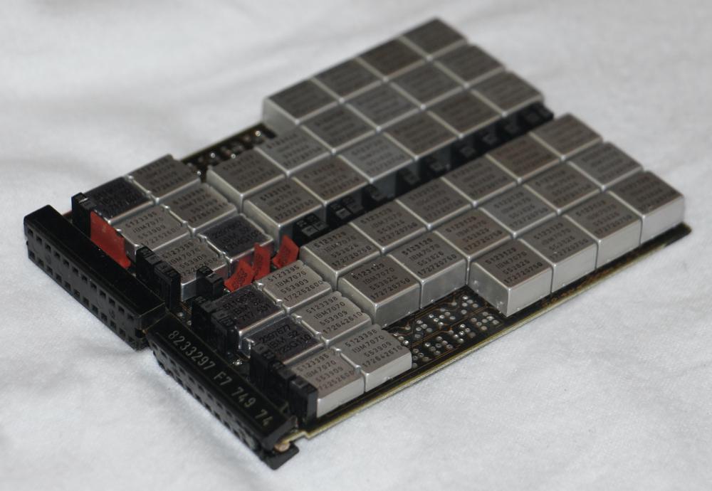
Each memory card (below) contained 32 of these modules to provide 32 kilobytes of storage. In the photo below, you can see the double-height memory modules along with shorter modules for support circuitry. A four-megabyte main memory unit held 144 of these cards in a frame about 3 feet × 3 feet × 1 foot, so semiconductor memory was still fairly bulky in 1972.
The memory board contains regular MST modules and double-height modules that hold the memory chips.
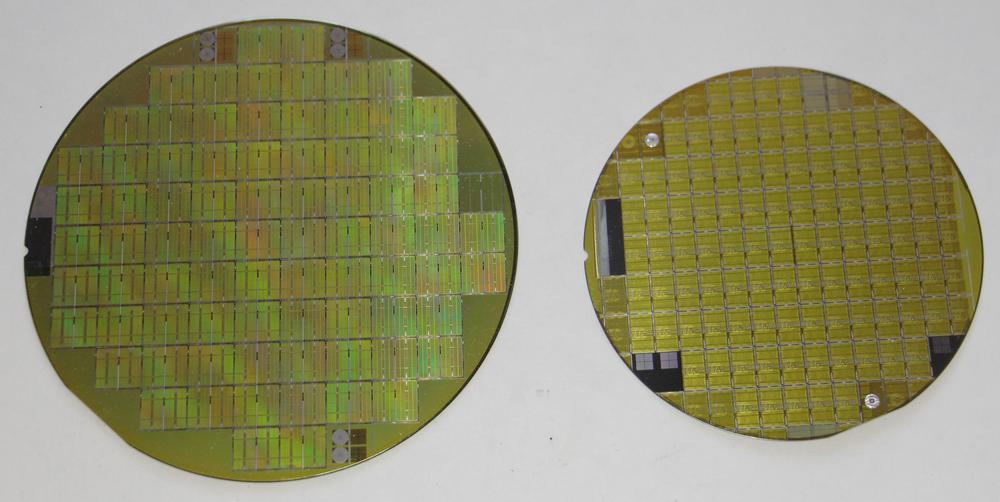
Moving along to some different memory chips, the box includes two silicon wafers holding memory dies, a 5" wafer and a 4" wafer.
The two silicon wafers.
The smaller four-inch wafer (1982) holds 288-kilobit dynamic RAM chips, an unusual size as it isn't a power of 2.15 The explanation is that the chip holds 32 kilobytes of 9-bit bytes (8 + parity). In the die photo, you can see that the memory array is mostly obscured by complex wiring on top of the die. This wiring is due to another unusual part of the chip's design: for the most efficient layout, the memory bit lines have a different spacing from the bit decode lines. As a result, irregular wiring is required to connect the parts of the chip together, forming the pattern visible on top of the chip. Because this die is on the wafer, you can see the alignment marks and test circuitry around the outside of the chip.
Die photo of the 4" wafer.
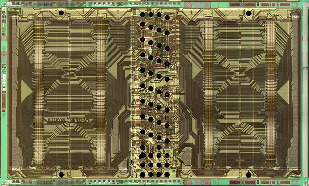
The five-inch wafer holds 1-megabit memory chips16 that were used in the IBM 3090 mainframe17 (1985). This computer used circuit cards with 32 of these chips, providing four megabytes of storage per card, a huge improvement over the 32-kilobyte card described earlier. The 3090 used multiple memory cards, providing up to 256 megabytes of main storage. The die photo below shows how the chip consists of 16 rectangular subarrays, each holding 64 kilobits.
Die photo of the 1-megabit DRAM chip on the 5" wafer. The dark circles are dirt, not solder balls.
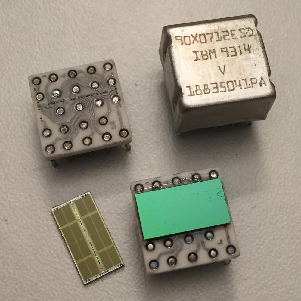
The photo below shows how this die is mounted upside-down on the ceramic substrate with the solder bumps connected to the 23 pins of the module. This module (not part of the box) was used in the IBM PS/2 personal computer.18 The die below looks green, unlike the die above, but that's just due to the lighting.
Construction of an IBM memory module. This module was not part of the box, but the die is the same as the 5" die. Photo courtesy of Antoine Bercovici.
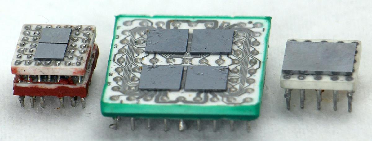
The photo below compares three memory modules from the technology box. The first module is the 8-kilobit module containing four 2-kilobit chips, described earlier. The second module is a much wider 512-kilobit module, built from four 128-kilobit dies. The third module contains a 1-megabit chip (the one in the 4-chip display, not from the wafer). These megabit modules were used in the IBM 3090 mainframe's secondary storage.
Three memory modules: 8-kilobit, 512-kilobit, and 1-megabit.
Disk platter
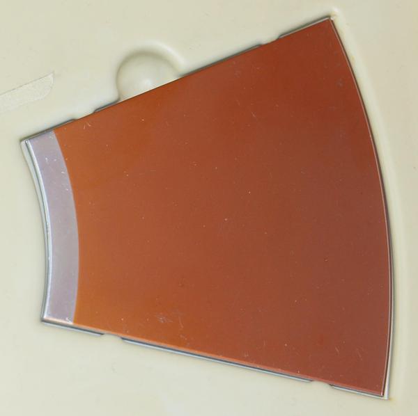
The box contains a segment of a 14" IBM disk platter, used in disk storage systems from minicomputers to mainframes. IBM was a pioneer in hard disks, starting with the IBM RAMAC (1956), which weighed over a ton and held 5 million characters on a stack of 24" platters. IBM switched to 14" platters in 1961 and by 1980 the IBM 3380 disk system held up to 2.5 gigabytes in a large cabinet of 14" platters.19 The 14" platter was also popular in low-cost, removable disk cartridge (1965) used with many minicomputers. The 14" disk platter was finally replaced by an 11" platter with the introduction of the IBM 3390 disk drive in 1989. Nowadays, laptops typically use 2.5" platters; amazingly, disk capacity kept increasing as disk diameter steeply decreased.
Section of a 14" disk platter from the display box.
Artifacts from the IBM 3090
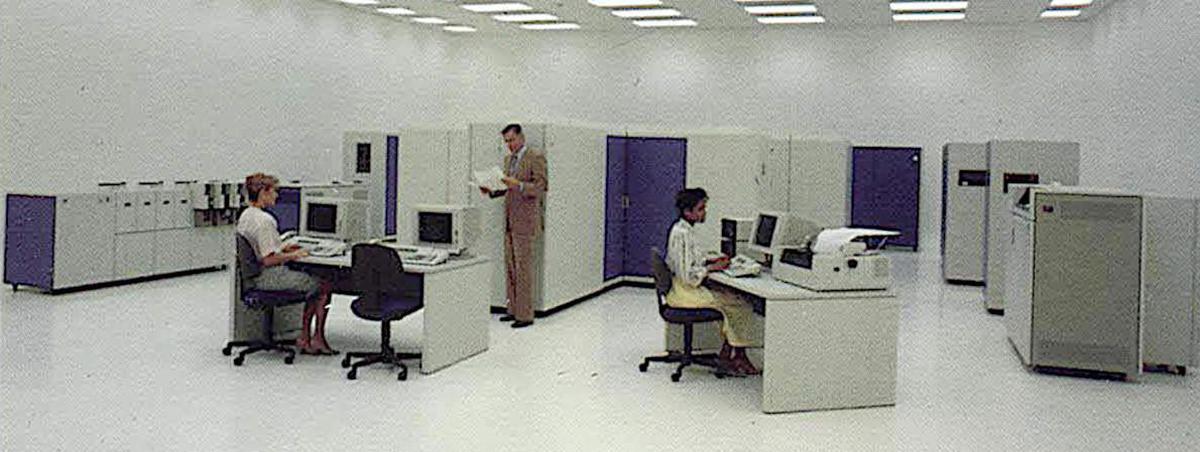
At the time of the box's creation, the 3090 mainframe was IBM's new high-performance computer (below), so the box has several artifacts that show off the technology in this computer. Although the IBM 3090 (1985) had top-of-the-line performance at the time, by 1998 an Intel Pentium II Xeon microprocessor had comparable performance,20 illustrating the remarkable improvements of microprocessor technology.
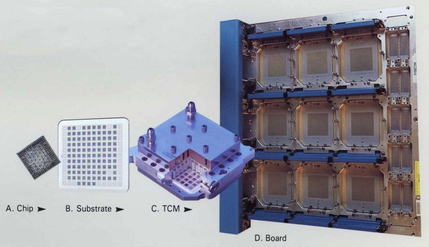
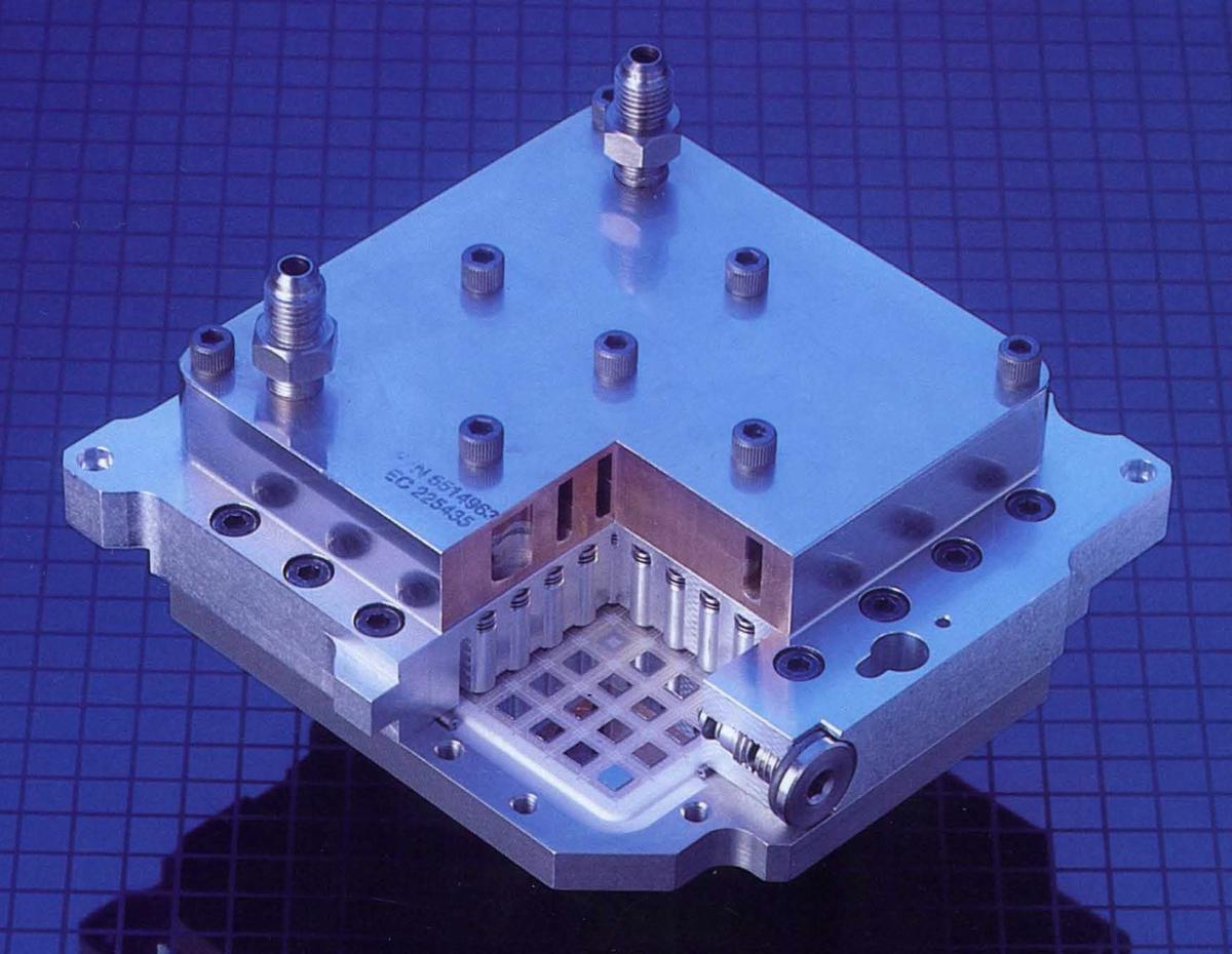
In 1980, IBM introduced the thermal conduction module (TCM), an advanced way to package integrated circuits at high density, while removing the heat that they generate.21 A TCM starts with a multi-chip module with about 100 high-speed integrated circuits mounted on a ceramic substrate, as shown below. This substrate contains dozens of wiring layers to connect the integrated circuits.22 To remove the heat, the ceramic substrate is packaged in a TCM, which has a metal piston contacting each silicon die. These pistons are surrounded by helium (which conducts heat better than air), and the whole TCM package is water-cooled. Finally, nine TCMs are mounted on a printed circuit board.
The hierarchy of components in the IBM 3090: chips are mounted on a ceramic substrate, which is assembled into a TCM. A board holds nine TCMs.
This incredibly complex heat-removal system was required because the 3090 used emitter-coupled logic (ECL), the same type of circuitry used in the Cray-1 supercomputer. Although ECL is a very fast logic family, it is also power-hungry and generates much more heat than the MOS transistors used in microprocessors.
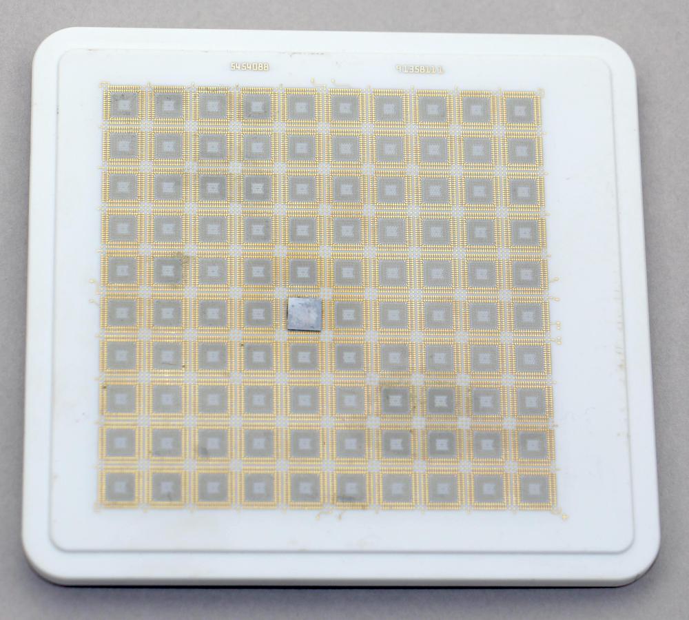
The ceramic substrate for a TCM, from the box. It is fairly small, measuring 11×11.7 cm. This substrate holds 100 silicon dies; one is visible near the middle.
The photo above shows the ceramic substrate. Normally, the substrate has 100 silicon dies mounted on it, but this sample has just a single die. The box also includes a cross-section slice of the ceramic substrate (below). This shows the 38 layers of wiring inside the substrate, as well as the pins on the underside.
Cross-section of the ceramic substrate, showing the multiple layers of internal wiring.
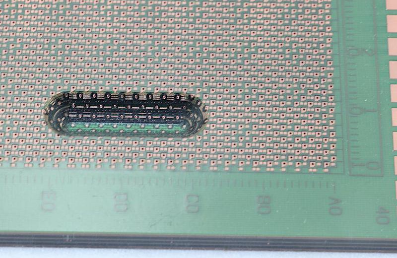
Each TCM had 1800 pins so it could be plugged into a printed circuit board and connected to the rest of the system. Each board held 9 TCMs and was powered with an incredible 1400 amps. The box includes a PCB sample, showing its multi-layer construction (below), and the dense grid of holes to receive the ceramic substrate.
Closeup of the printed circuit board used in the IBM 3090. The routed groove shows the multi-layer construction.
Finally, here's a nice cutaway of a TCM from the detailed IBM 3090 brochure. At the bottom, it shows the silicon dies mounted on the ceramic substrate. The dies are contacted by the heat sink pistons in the middle. The connections on top are for the cooling water.
This cut-away image from IBM shows the internal construction of a TCM.
Conclusion
This technology exhibit box was created 35 years ago. Looking at it from the present provides a perspective on the history of both IBM and the computer industry. The box's date, 1986, marks the peak of IBM's success and influence,23 right before microcomputers decimated the mainframe market and IBM's dominance. What I find interesting is that the technology box focuses on mainframes and lacks any artifacts from the IBM PC (1981), which ended up having much more long-term impact..24 This neglect of microcomputers reflects IBM's corporate focus on the mainframe market rather than the PC market (which, ironically, IBM created).
In the bigger historical picture, the technology box covers a time of great upheaval as electromechanical accounting machines were replaced by three generations of computers in rapid succession: vacuums tubes, then transistors, and finally integrated circuits. In contrast to this period of rapid change, nothing has replaced integrated circuits over the past 50 years. Instead, integrated circuits have remained, but improved by many orders of magnitude, as described by Moore's Law. (Compared to the room-filling IBM 3090 mainframe, an iPhone has 1000 times the performance and 50 times the RAM.) Will integrated circuits continue their dominance for the next 50 years or will some new technology replace them? It remains to be seen.
Thanks to Cyprien for providing this amazing box of artifacts. I announce my latest blog posts on Twitter, so follow me @kenshirriff. I also have an RSS feed.
Notes and references
from Hacker News https://ift.tt/39XAOnR



No comments:
Post a Comment
Note: Only a member of this blog may post a comment.