Introduction
The PCI Express® (PCIe®) architecture has served as the backbone for I/O connectivity spanning three decades, enabling power-efficient, high-bandwidth, and low-latency communication between components. PCI Express technology just debuted its sixth generation at 64.0 GT/s, as part of its evolution, doubling the bandwidth every generation, while maintaining full backwards compatibility (Figure 1). PCIe technology continues to outpace competing I/O technologies in terms of market share, capacity, and bandwidth and has continued as the ubiquitous I/O interconnect across the entire compute continuum through its existence. Its usage spans diverse market segments such as hand-held, client, servers, workstations, data centers, High performance computing, automotive, embedded systems, industrial applications, etc. PCIe technology is so pervasive with its compelling power-efficient performance and cost effectiveness that other protocols including ultra-latency sensitive load-store I/O protocols with memory, storage, and coherency semantics (e.g., Compute Express Link – CXL®, NVM Express®) run on PCIe PHY and leverage the PCIe infrastructure such as upper layers, software stack and platform connectivity.

Figure 1: PCIe specification evolution through six generations spanning three decades: Doubling Bandwidth with leading power-efficient and cost-effective performance satisfying the needs across the entire compute continuum as the ubiquitous interconnect
PCI-SIG®, a consortium of about 900 member companies, owns, manages and develops PCIe technology as an open industry standard. In order to address the insatiable bandwidth demand of emerging applications such as Artificial Intelligence, Machine Learning, networking, communication systems, storage, and High-Performance Computing, PCI-SIG just released the sixth generation of PCIe technology. The purpose of this white paper is to provide insights into the technical analysis and trade-offs that were considered for PCIe 6.0 specification in order to deliver cost-effective, scalable and power-efficient performance in a backwards compatible manner.
PCIe 6.0 Requirements
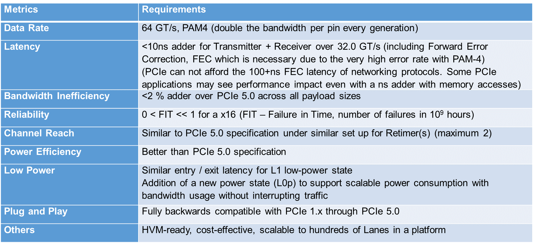
PCI Express is a Load-Store interconnect with challenging latency, bandwidth and power requirements. Several segments that deploy PCIe technology also have very stringent requirements in reliability and cost. As a ubiquitous I/O, PCIe architecture needs to meet these requirements across the entire compute continuum, with full backwards compatibility, as detailed in Table 1 below.
Table 1: PCIe 6.0 Specification Target Requirements to satisfy the needs of all platforms where PCIe technology is deployed

Error Model with PAM4 Signaling
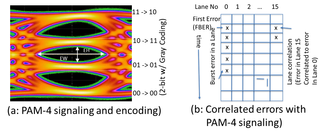
PCIe 6.0 specification requires significant improvements to the package, connectors, and the materials, as we have done with prior speed increases. In addition to the channel improvements, PCIe 6.0 specification uses PAM4 (Pulse Amplitude Modulation, 4 levels) signaling to achieve similar channel reach as PCIe 5.0 specification. PAM4 uses 4 voltage levels to encode 2 bits of data, as shown in Figure 2, while running the clock at the same 16G Nyquist frequency as PCIe 5.0 specification. While PAM4 helps with the channel reach, it comes at the expense of much higher bit error rate (BER), which has been 10-12 for the first five generations of PCIe specifications. BER is the measure of the number of bit errors in the Receiver divided by the total number of bits received. With PAM4 signaling, errors are expected to occur in clusters, as shown in Fig. 2. When a bit error happens, the decision feedback equalizer (DFE) in a Receiver may induce errors in subsequent bits due to propagation of feedback from the prior bit error(s), resulting in burst errors. While the number of errors in a burst as well as the length of the burst can be mitigated by techniques such as proper selection of PHY equalization methods, gray-coding of the 4-levels of PAM4, and precoding, the burst errors in a Lane need to be addressed. Other forms of correlation across Lanes in a Link are also possible due to common noise sources such as power supply noise.

Figure 2: PAM4 signaling and burst error in a Lane due to DFE as well as correlated errors across Lanes due to common noise sources
Error Handling with PCIe 6.0 Architecture at 64.0 GT/s
With PAM4 encoding, the bit error rate (BER) at 64.0 GT/s is expected to be several orders of magnitude worse than the BER of 10-12 that existed in the past 5 generations of PCIe specifications. Even though PCIe architecture has a Link Level retry (LLR) mechanism to replay transactions impacted by error(s), the loss of bandwidth due to retry makes it untenable with PAM4 error rates. Thus, PCIe 6.0 specification uses a light-weight FEC in conjunction with the LLR mechanism to meet the performance metrics of low latency and low bandwidth overhead delineated in Table 1.

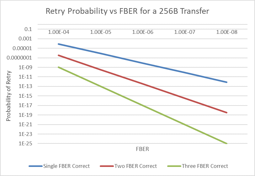
Figure 3: Retry Probability vs. FBER for a 256B transfer for a x1 Link, assuming each FBER instance is assumed to be a Symbol that can be corrected by the FEC. This demonstrates that a single FBER correct FEC with an FBER of 10-6 combined with a low-latency replay mechanism is the best solution to meet the stringent latency requirements of PCIe applications. Even a two FBER correct FEC would have resulted in a latency increase in the range of tens of nsecs.
PCIe 6.0 specification defines a parameter called `FBER’ (First Bit Error Rate). It is the probability of a (first) bit error occurring at the Receiver pin. An FBER occurrence may cause other correlated errors, as shown in Figure 2b. All those individual correlated errors count as one from an FBER count perspective. We have extensively studied the trade-offs associated between FBER along with error correlation on FIT, retry probability, and bandwidth loss due to retry, for different FEC capabilities. A simple study for a x1 Link is shown in Figure 3 as an illustration. As expected, the retry probability decreases with the number of FBER instances that can be corrected with an 256-byte payload. However, retry probability decreases exponentially with the decrease in FBER. A stronger FEC results in higher latency as the complexity increases exponentially with the number of Symbols corrected. On the other hand, a lower FBER results in reduced channel reach. We chose a 3-way interleaved single Symbol correct FEC (as shown later in Figure 4) to correct a single FBER instance with an FBER of 10-6 in order to have an acceptable retry probability in the 10-5 range. This light-weight causes the FEC correction latency to be less than 2ns. The lower FBER of 10-6 (vs the 10-4 in networking standards) does result in shorter channel reach by about 2-4 inches. However, in spite of this channel length trade-off, we are still within the channel reach of existing channels. Further, over time, we have seen constant improvements in packages, materials, and connectors, resulting in longer channel reach whereas the latency impact due to a stronger FEC does not change over time. Thus, with our choice of light-weight FEC and a slightly stringent FBER, we have made the right trade-offs to stay flat on latency while meeting the existing channel reach requirements backed by rigorous analysis and silicon data.
Our studies also demonstrated the need for a strong CRC to achieve the reliability goals of a very low FIT due to counter the high rate of errors with correlation. We chose a 64-bit CRC to protect every 256 bytes. Our CRC is based on the Reed-solomon code with g(x) = (x+α)(x+α2)… (x+α8), where α is the root of a primitive polynomial over GF(28). This offers a very robust error detection mechanism since it is guaranteed to detect up to 8 Bytes in error (post-FEC) and has an aliasing probability of 2-64 beyond that. The CRC complexity increases logarithmically with the number of bits since we are only checking if a syndrome is zero. Thus, the increased number of CRC bits has a negligible impact on the gate count or the latency. Thus, the light-weight FEC delivers a received packet with an error probability of about 10-5 whereas the strong CRC practically guarantees that an erroneous packet will be detected (with a FIT close to 0, as shown in Table 2) and a link layer replay will cause the packet to be retransmitted all within very tight low-latency constraints.
Flit Mode in PCIe 6.0 Specification
We need a fixed sized transfer entity (we call it a Flit which stands for flow control unit) that the FEC encode/ decode/ correction can be applied to. With a fixed Flit size, it is natural to have the CRC-based error detection as well as ack/nak and retry mechanism to operate at the Flit level.
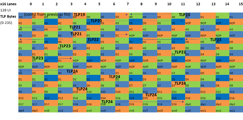
A Flit can have multiple packets (both Data Link Layer Packet – DLLP and Transaction Layer Packet- TLP) and a TLP/DLLP may span across multiple Flits (as shown in Figure 4). Since the Flit includes the CRC, the DLLP and TLP do not carry their individual CRC bytes as they did in prior generations. We have also removed the PHY layer Framing Token for every TLP or DLLP, due to the fixed position of TLP/ DLLPs within a Flit. The fixed DLLP bytes helps with a predictable low-latency replay mechanism and reduces queuing overheads. These mechanisms help boost link efficiency to overcome the FEC and CRC overhead.
A Flit comprises of 256 bytes. Each byte is sent on one Lane and bytes are interleaved across the width of the Link, consistent with the layout in prior generations. The first 236 bytes of the flit are for TLP(s), followed by 6 bytes for Data Link Layer Payload (DLP), followed by 8 bytes for CRC covering the first 242 bytes of TLP and DLP, followed by 6 bytes of FEC, covering the entire Flit.

Figure 4: TLP arrangement in a Flit in a x16 Link
Three single Symbol correct capable FEC groups are interleaved across consecutive bytes, as shown using different color combinations in Figure 4. Each color is a different FEC group, comprising of 85B, 85B, and 84B respectively. Due to this 3-way FEC interleaving, no burst error can affect two Symbols of the same FEC group, as long as the burst length is <= 16. Thus, one occurrence of FBER in a flit can be corrected if the burst length is <=16 and we get no correlation errors across Lanes. PCIe 6.0 specification ensures that the burst length > 16 occurs with a probability less than FBER by constraining the DFE (Decision Feedback Equalizer) tap weights and balancing the Transmitter Equalization (TxEQ), the CTLE (Continuous Time Linear Equalization) and DFE equalization parameters. Other techniques such as gray coding and precoding have been deployed to mitigate the effect of correlated errors. Extensive analysis has been deployed to ensure that this requirement can be met across the wide range of channels across different platforms where PCIe technology is deployed.
Performance and Reliability Results
We present the various metrics in this section. Detailed mathematical analysis of the results presented here can be found in our 2021 IEEE Hot Interconnects paper.
Table 2 demonstrates that the retry probability and bandwidth loss is within expectation. Unlike prior generations, Flit retry will be common with 64.0 GT/s data rate, although their impact on bandwidth will be minimal. Furthermore, with the expected retry time of about 100ns, we do not expect to see much jitter since it is a fraction of the total access time and the queuing delays in a loaded system will far exceed that additional latency in case of a retry.
Table 2: Retry Probability, B/W loss, and FIT as a function of FBER and Retry time based on the FEC/ CRC for a x16 Link. The 10-5 FBER column is provided to demonstrate that it is not a viable solution point with a bandwidth loss of about 5%. Retries will be common with PCIe 6.0 architecture but with the low retry time, the performance impact will not be noticeable.
|
FBER/ Retry Time |
10-6/ 100ns |
10-6/ 200ns |
10-6/ 300ns |
10-5/ 200ns |
|
Retry probability per flit |
5 x 10⁻⁶ |
5 x 10⁻⁶ |
5 x 10⁻⁶ |
0.048 |
|
B/W loss with go-back-n (%) |
0.025 |
0.05 |
0.075 |
4.8 |
|
FIT |
4 x 10⁻⁷ |
4 x 10⁻⁷ |
4 x 10⁻⁷ |
4 x 10⁻⁴ |
Figure 5 shows the bandwidth scaling of Flit mode at 64.0 GT/s vs the 128b/130b encoding at 32.0 GT/s. The packet efficiency of Flit mode exceeds that of the 128b/130b encoding for payloads up to 512 Bytes (32 DWs), resulting in an up to ~3X improvement in effective throughput for smaller payloads (2X from data rate increase and ~1.5X improvement in bandwidth efficiency). As the TLP size increases, this efficiency goes down and for the 4KB data payload size, it reduces to 0.98, in line with the bandwidth inefficiency provided in the metrics of Table 1.
Figure 5: Bandwidth scaling with Flit Mode at 64.0 GT/s over 128b/130b encoding at 32.0 GT/s. For practical systems, we expect to see more than 2X useable bandwidth with PCIe 6.0 specification at 64.0 GT/s over the 32.0 GT/s with PCIe 5.0 specification
The measured latency in the Flit Mode is lower at 64.0 GT/s than the prior generations except for lower link widths (x1/ x2) and TLPs with small payload sizes (<= 16 B). The higher data rate results in faster transmission time of a packet. Removal of PHY encoding mechanisms such as Framing Token and Sync header further reduces the latency. For example, a TLP with a 256-B payload will see a latency reduction greater than 1ns. Even for a x1 Link transmitting a 3DW TLP, the increase in latency is expected to be less than 10ns, meeting the requirements of Table 1.
Conclusions
We have demonstrated that PCIe 6.0 specification meets or exceeds all the requirements of Table 1. An interconnect technology is considered successful if it can sustain three generations of bandwidth improvement spanning a decade. PCIe architecture has far exceeded that mark. As we embark on the third decade, PCIe technology is looking strong as the ubiquitous I/O interconnect over the entire compute continuum. As the industry continues its journey to the sixth generation of PCIe specification, it will benefit from the power-efficient performance it will deliver in a High Volume Manufacturing (HVM) environment with hundreds of Lanes connecting multiple devices in a platform.
About PCI-SIG
PCI-SIG is the consortium that owns and manages PCI specifications as open industry standards. The organization defines industry standard I/O (input/output) specifications consistent with the needs of its members. Currently, PCI-SIG is comprised of about 900 industry-leading member companies. To join PCI-SIG, and for a list of the Board of Directors, visit www.pcisig.com.
PCI-SIG, PCI Express, and PCIe are trademarks or registered trademarks of PCI-SIG. All other trademarks are the property of their respective owners.
from Hacker News https://ift.tt/3Fpn6b7
No comments:
Post a Comment
Note: Only a member of this blog may post a comment.