Backstory and first attempts
As I mentioned in my last post I’ve been working on reverse engineering the PLA chip in the C128. I’m now mostly done with this process so I think it’s time to share some of the findings.
This has been a very interesting project as I did not really know much about semiconductor design and manufacturing. My existing knowledge extended to having seen some die shots and admiring the pretty looking pictures.
It all started with me buying a cheap microscope to help with soldering surface mount components.
Some time later I ended up watching a video on youtube showing a simpler way of getting silicon dies out of the packaging.
This looked simple enough to try at home as I already had all the equipment needed. Decapping an IC usually involves heated sulphuric acid or other similar nasty chemicals which I do not really want to play with at home. So I dug out a couple of broken MOS chips I had lying around (never throw things away, could come in handy). After fiddling around a bit I ended up with two 8521R0 dies and one 8721 PLA. The first real photo was the one show in the last post.
Better microscope
While this was a success I quickly realised that this microscope did not have enough resolution for me to be able to capture images of high enough quality. The maximum magnification is 90x, when using a 2x barlow lens. Additionally it does not have a stage so I had to place the die on a table and then move the whole microscope, which is very unstable and makes it hard to capture the bits you want to see.
As such a better microscope was sourced and purchased, still within reasonable money.
This proved to be much better at taking pictures of decent quality, I was however not happy with the camera I bought with it. It’s a cheap camera with no capability for me to manage it remotely except using the AmScope application. Around this time, the Raspberry Pi foundation released the new High Quality camera for the Raspberry Pi. This camera has a C-mount on it which matches the microscope so I quickly bought one and put in on the microscope. This camera is fantastic for this job, full control of the whole process from the comfort of linux.
All in all a vast improvement to the previous setup. With the higher resolution I started needing to stitch the photos together to make larger pictures. This sounded simple at the start and ended up being (as you can probably guess) not very easy at all. I’m still struggling with the stitching, but slowly improving. One of the key things for a successful panorama stitch is to have consistent photos when it comes to panning, focus, white balance etc. etc. The more even the photos, the easier and better the stitching becomes.
Motorizing
This led me to start working on motorizing the table. It was getting really tiresome having to manually move the table around and the photos ended up being moved in multiple axis etc.
Lots of design work, 3D printing and research into CNC firmwares later I ended up with the following setup:
Going from the top we have a Raspberry 7” display, with a Raspberry Pi4 mounted on the back. Not see is also the RPi HiQ camera mounted on the microscope. The RPi takes photos, displays previews on the display and also runs the python code that controls the CNC board.
The stage and the levelling table is motorized with 28BYJ-48 steppers controlled using a small board with an ESP32 running Grbl_Esp32 and four AD4498 stepper motor controllers.
This whole setup has some issues both in software and hardware but it works well enough for now to enable me to do some work.
Putting chips in reverse
With the logistics now sorted out I returned to the work of reverse engineering the chip itself. My initial focus was on the PLA chip as this should be one of the simpler ones to figure out. PLA stands for Programmable Logic Array and is a very common structure in designs from this era.
Looking at the schematic diagram from wikipedia we should expect to see two main arrays, AND and OR. Inputs are connected to AND and outputs from the OR array.
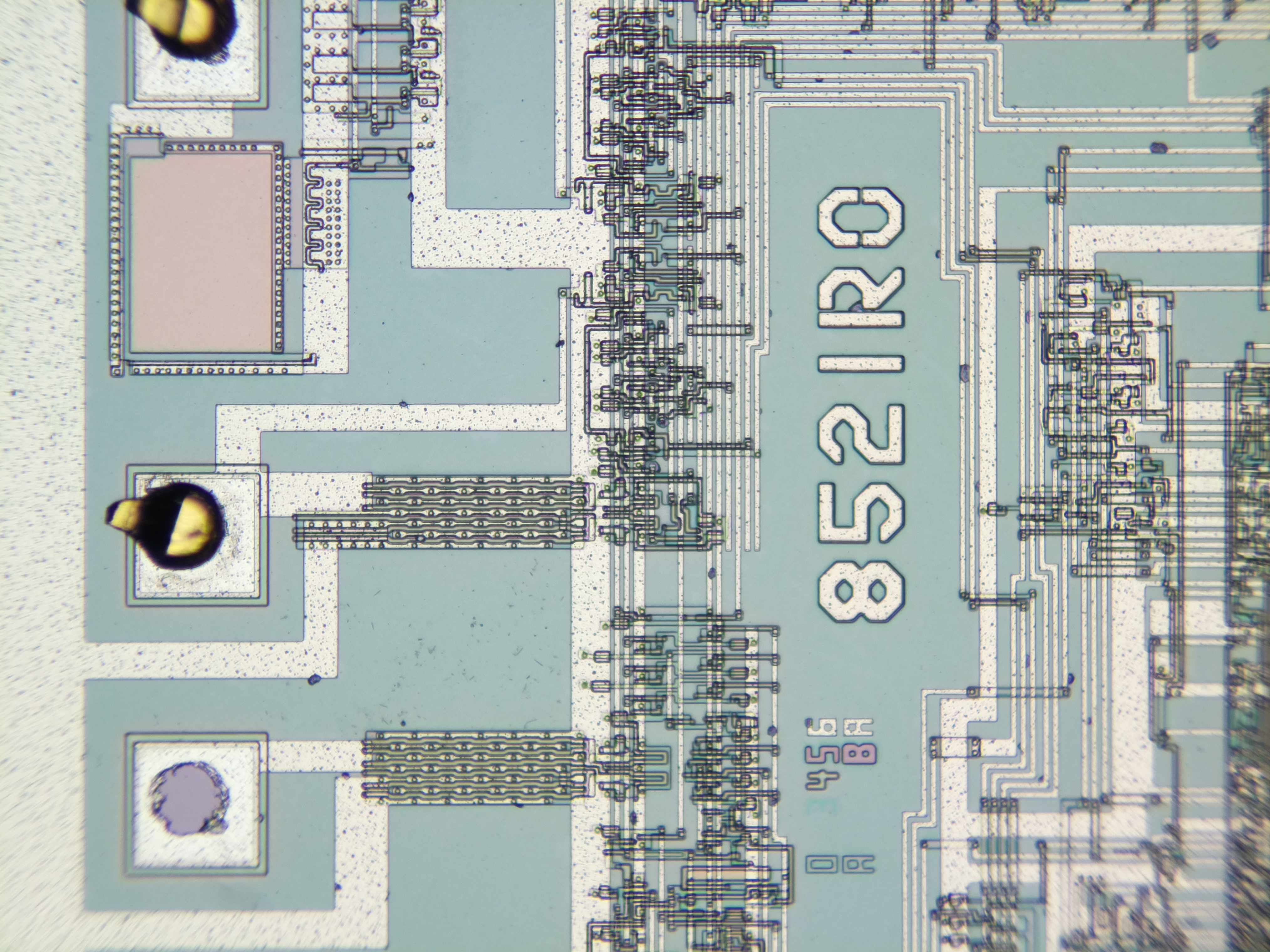
Going back to the previous die shot with can improve it with some annotations for the pins and the general areas of the chip. Once we have established the pins we can see that all the inputs are connected to one array and all the outputs to the other array, just as expected. This also helps us establish which array is which.
Here we see the I/O pins marked up with how they are connected to the lead frame and the pins on the DIP itself. We can also see the two main areas that make up a PLA structure, the AND array and the OR array. Additionally there is some extra logic at the bottom marked with a question mark. The function of this was unknown to me but as all the output pins are passing through it I was guessing that it was an output stage of some kind.
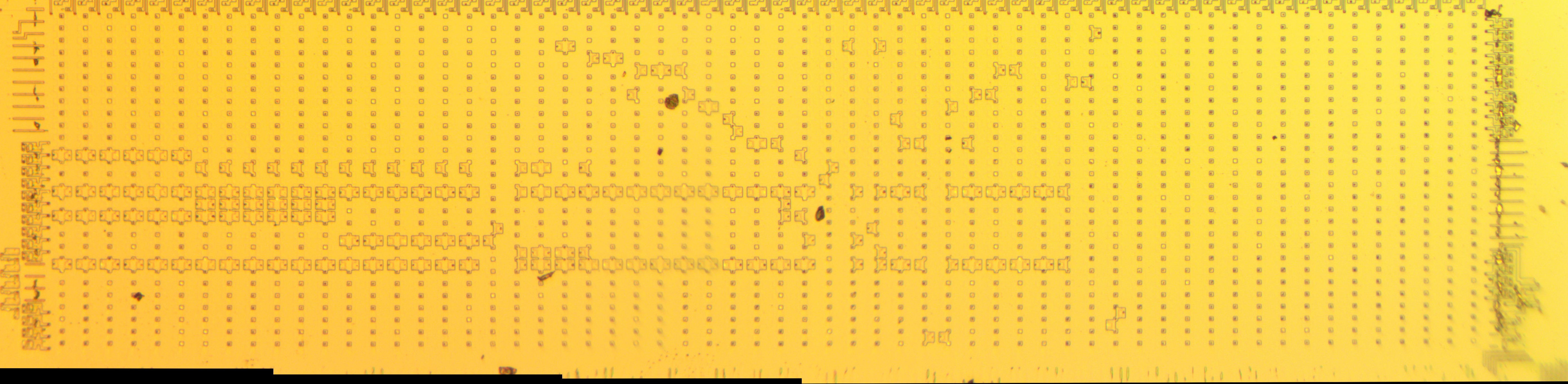
AND array
So, if we take a closer look at the AND matrix to start with we will see the following. The colours are a bit off as this was still done using the AmScope camera and I didn’t figure out how to set the white balance on it.
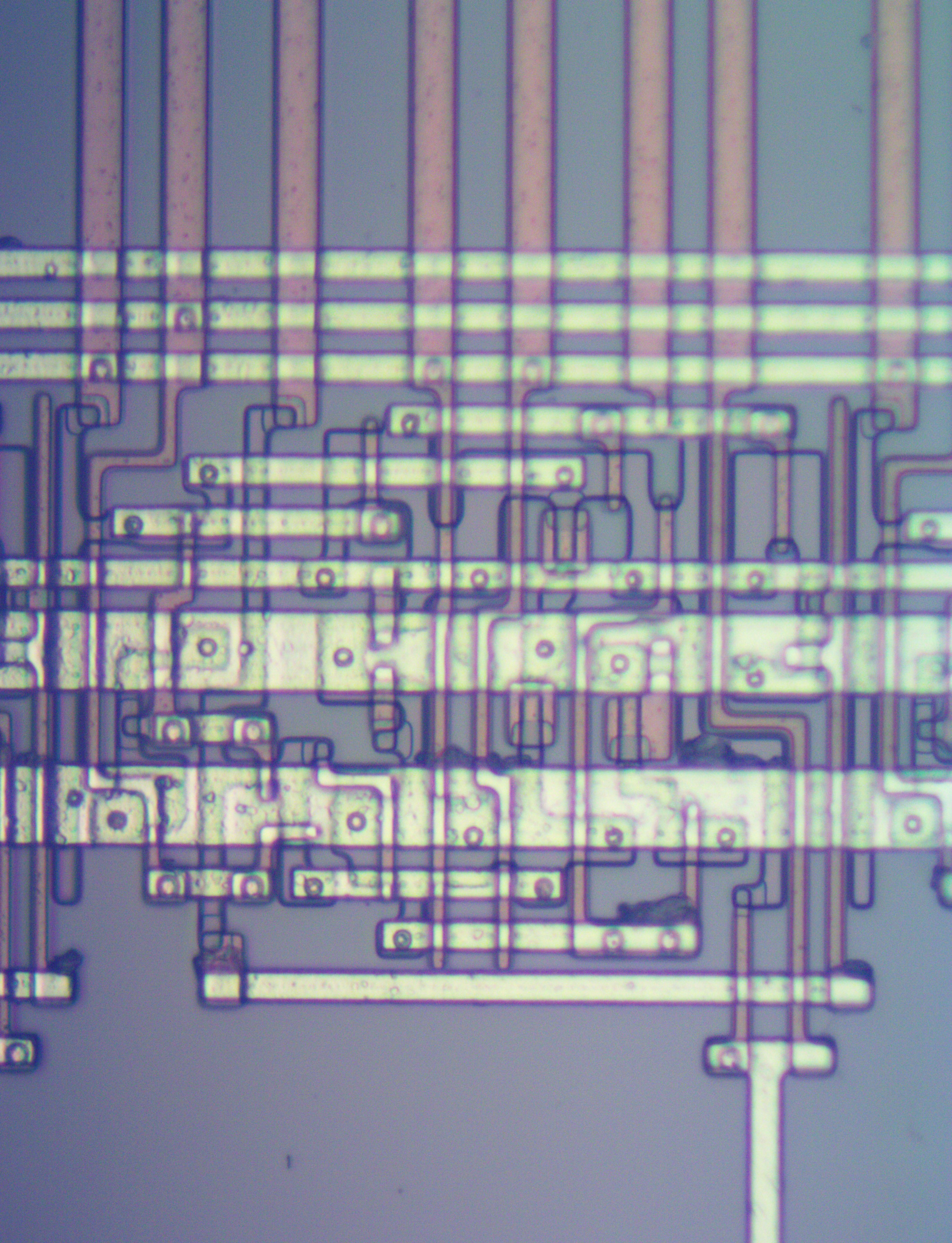
This was not very helpful to understand what was going on as all the interesting bits are covered up by the top-most metal layer. This was early on when I was still learning a lot so to remove the metal I took a very brute force approach. I use heavy mechanical scrubbing to remove the metal which I also learned once I put it back in the microscope had removed everything but the substrate itself. Oops.
Fortunately, the details that I needed were in the diffusion embedded into the substrate:
Looking closely at this image we can see little squiggly lines where a transistor is located to create a connection within the matrix.
OR array
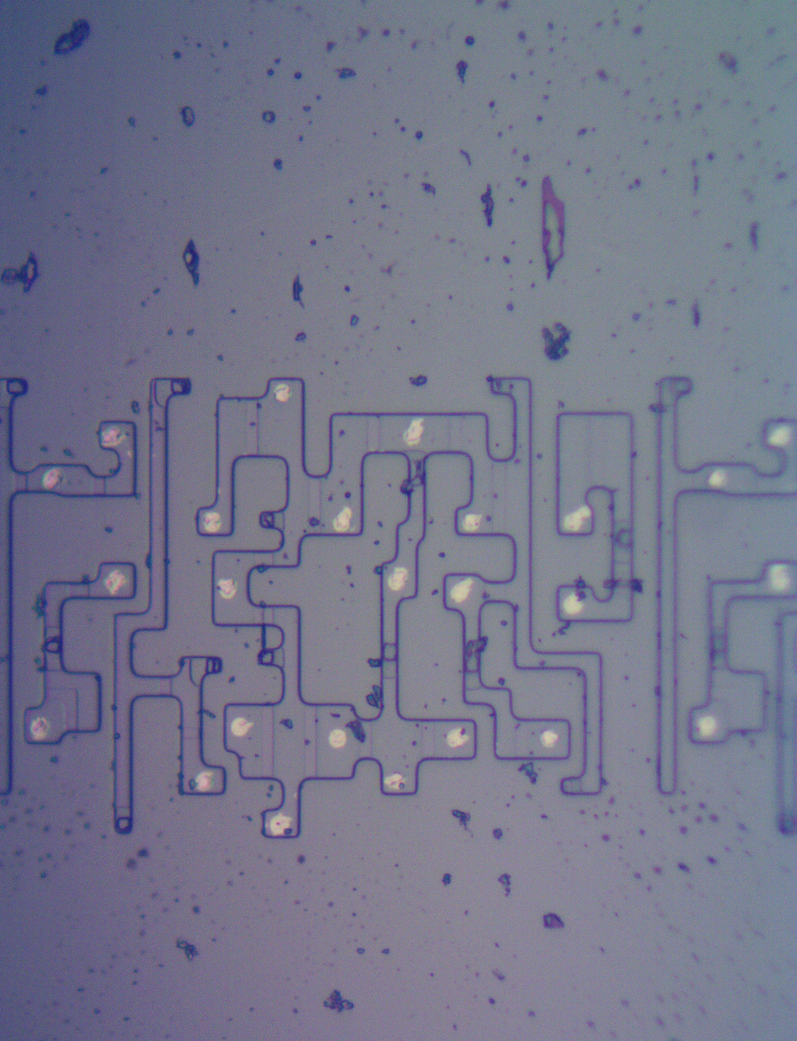
Moving on to the OR array we see the exact same pattern. Hard to tell with the metal layer in place, though easier compared to the AND matrix. Much easier with just the substrate and diffusion left.

Full matrix decode
Armed with this knowledge we can now proceed with extracting the full PLA logic matrix from the images.
I marked all transistors in each matrix with a dot and got the following picture:
All inputs are horizontal in the AND matrix, with each line having a normal and an inverted signal being fed in. All outputs are horizontal in the OR matrix and they are connected with vertical lines called product terms.
By looking at the dots, we can decode the product terms by doing logic and for all vertical lines in the AND matrix, for example
p0 = CHAREN & HIRAM & BA & !MS3 & GAME & RW & AEC & A12 & !A13 & A14 & A15
For the outputs we instead look horizontal for each output and combine with or, for example
SDEN = p42 | p43 | p66 | p69
So now we have the entire set of logic equations. Hooray!
Output stage
Going back to the full die picture, we now have everything but the box marked with a question mark in the output path.
Looking at higher resolution photos of this we can see similar structures for each output. In all cases except two the structure is bypassed and the output from the OR matrix goes directly to the output pin. This is however not the case for the two pins DWE and CASENB.
DWE is the Write Enable signal going to the main system DRAM chips, CASENB is gating the CAS signal towards the RAM. These two signals are processed in some form using these output gate structures, so I had to reverse engineer this block.
After quite some time reading up on silicon chip design and manufacturing and a lot of attempts I managed to come up with a schematic for this that makes sense. I’m not going to go into the whole process here but I will document and post it later. Here I would also like to thank Frank Wolf for his help, please support his project if you can!
Going a bit further, the way this is used in the DWE and CASENB outputs makes it a normal D-latch. The latch enable for this also comes for the PLA matrix in a pair of lines in the OR matrix.
Result
So as a final result we can now write down the full HDL code for the C128 PLA chip. I’m using verilog for this. Mind you this is the first verilog I’ve ever written so it’s probably suboptimal. Using a D-latch for the output in verilog is normally seen as a bad thing, however in this case I am doing it to replicate the logic and function of the existing chip.
I have validated this to the best of my knowledge, but if I’ve missed anything please let me know!
In difference to the C64 PLA the C128 PLA can not be replaced with just an EPROM or similar due to the presence of the output latches.
module pla_8721(
    input rom_256,
    input va14,
    input charen,
    input hiram,
    input loram,
    input ba,
    input vma5,
    input vma4,
    input ms0,
    input ms1,
    input ms2,
    input ms3,
    input z80io,
    input z80en,
    input exrom,
    input game,
    input rw,
    input aec,
    input dmaack,
    input vicfix,
    input a10,
    input a11,
    input a12,
    input a13,
    input a14,
    input a15,
    input clk,

    output sden,
    output roml,
    output romh,
    output clrbnk,
    output from,
    output rom4,
    output rom3,
    output rom2,
    output rom1,
    output iocs,
    output dir,
    output reg dwe,
    output reg casenb,
    output vic,
    output ioacc,
    output gwe,
    output colram,
    output charom);

wire p0;
wire p1;
wire p2;
wire p3;
wire p4;
wire p5;
wire p6;
wire p7;
wire p8;
wire p9;
wire p10;
wire p11;
wire p12;
wire p13;
wire p14;
wire p15;
wire p16;
wire p17;
wire p18;
wire p19;
wire p20;
wire p21;
wire p22;
wire p23;
wire p24;
wire p25;
wire p26;
wire p27;
wire p28;
wire p29;
wire p30;
wire p31;
wire p32;
wire p33;
wire p34;
wire p35;
wire p36;
wire p37;
wire p38;
wire p39;
wire p40;
wire p41;
wire p42;
wire p43;
wire p44;
wire p45;
wire p46;
wire p47;
wire p48;
wire p49;
wire p50;
wire p51;
wire p52;
wire p53;
wire p54;
wire p55;
wire p56;
wire p57;
wire p58;
wire p59;
wire p60;
wire p61;
wire p62;
wire p63;
wire p64;
wire p65;
wire p66;
wire p67;
wire p68;
wire p69;
wire p70;
wire p71;
wire p72;
wire p73;
wire p74;
wire p75;
wire p76;
wire p77;
wire p78;
wire p79;
wire p80;
wire p81;
wire p82;
wire p83;
wire p84;
wire p85;
wire p86;
wire p87;
wire p88;
wire p89;

wire casenb_int;
wire casenb_latch;

/* Product terms */

assign p0 = charen & hiram & ba & !ms3 & game &  rw & aec & a12 & !a13 & a14 & a15;
assign p1 = charen & hiram &      !ms3 & game & !rw & aec & a12 & !a13 & a14 & a15;
assign p2 = charen & loram & ba & !ms3 & game &  rw & aec & a12 & !a13 & a14 & a15;
assign p3 = charen & loram &      !ms3 & game & !rw & aec & a12 & !a13 & a14 & a15;

assign p4 = charen & hiram & ba & !ms3 & !exrom & !game &  rw & aec & a12 & !a13 & a14 & a15;
assign p5 = charen & hiram &      !ms3 & !exrom & !game & !rw & aec & a12 & !a13 & a14 & a15;
assign p6 = charen & loram & ba & !ms3 & !exrom & !game &  rw & aec & a12 & !a13 & a14 & a15;
assign p7 = charen & loram &      !ms3 & !exrom & !game & !rw & aec & a12 & !a13 & a14 & a15;

assign p8 = ba & !ms3 & exrom & !game & rw & aec & a13 & !a13 & a14 & a15;
assign p9 =      !ms3 & exrom & !game & rw & aec & a12 & !a13 & a14 & a15;

assign p10 = ba & !ms2 & ms3 &  rw & aec & a12 & !a13 & a14 & a15;
assign p11 =      !ms2 & ms3 & !rw & aec & a12 & !a13 & a14 & a15;

assign p12 = charen & hiram & ba & !ms3 & game &  rw & aec & !a10 & !a11 & a12 & !a13 & a14 & a15;
assign p13 = charen & hiram &      !ms3 & game & !rw & aec & !a10 & !a11 & a12 & !a13 & a14 & a15;
assign p14 = charen & loram & ba & !ms3 & game &  rw & aec & !a10 & !a11 & a12 & !a13 & a14 & a15;
assign p15 = charen & loram &      !ms3 & game & !rw & aec & !a10 & !a11 & a12 & !a13 & a14 & a15;

assign p16 = charen & hiram & ba & !ms3 & !exrom & !game &  rw & aec & !a10 & !a11 & a12 & !a13 & a14 & a15;
assign p17 = charen & hiram &      !ms3 & !exrom & !game & !rw & aec & !a10 & !a11 & a12 & !a13 & a14 & a15;
assign p18 = charen & loram & ba & !ms3 & !exrom & !game &  rw & aec & !a10 & !a11 & a12 & !a13 & a14 & a15;
assign p19 = charen & loram &      !ms3 & !exrom & !game & !rw & aec & !a10 & !a11 & a12 & !a13 & a14 & a15;

assign p20 = ba & !ms3 & exrom & !game & rw & aec & !a10 & !a11 & a12 & !a13 & a14 & a15;
assign p21 =      !ms3 & exrom & !game & rw & aec & !a10 & !a11 & a12 & !a13 & a14 & a15;

assign p22 = ba & !ms2 & ms3 &  rw & aec & !a10 & !a11 & a12 & !a13 & a14 & a15;
assign p23 =      !ms2 & ms3 & !rw & aec & !a10 & !a11 & a12 & !a13 & a14 & a15;

assign p24 = charen & hiram & ba & !ms3 & game &  rw & aec & !a10 & a11 & a12 & !a13 & a14 & a15;
assign p25 = charen & hiram &      !ms3 & game & !rw & aec & !a10 & a11 & a12 & !a13 & a14 & a15;
assign p26 = charen & loram & ba & !ms3 & game &  rw & aec & !a10 & a11 & a12 & !a13 & a14 & a15;
assign p27 = charen & loram &      !ms3 & game & !rw & aec & !a10 & a11 & a12 & !a13 & a14 & a15;

assign p28 = charen & hiram & ba & !ms3 & !exrom & !game &  rw & aec & !a10 & a11 & a12 & !a13 & a14 & a15;
assign p29 = charen & hiram &      !ms3 & !exrom & !game & !rw & aec & !a10 & a11 & a12 & !a13 & a14 & a15;
assign p30 = charen & loram & ba & !ms3 & !exrom & !game &  rw & aec & !a10 & a11 & a12 & !a13 & a14 & a15;
assign p31 = charen & loram &      !ms3 & !exrom & !game & !rw & aec & !a10 & a11 & a12 & !a13       & a15;

assign p32 = ba & !ms3 & exrom & !game & rw & aec & !a10 & a11 & a12 & !a13 & a14 & a15;
assign p33 =      !ms3 & exrom & !game & rw & aec & !a10 & a11 & a12 & !a13       & a15;

assign p34 = ba & !ms2 & ms3 &  rw & aec & !a10 & a11 & a12 & !a13 & a14 & a15;
assign p35 =      !ms2 & ms3 & !rw & aec & !a10 & a11 & a12 & !a13       & a15;

assign p36 = !aec;
assign p37 = !rw & aec & !a10 & a11 & a12 & !a13 & a15;

assign p39 = !charen & hiram & !ms3 &           game & rw & aec & a12 & !a13 & a14 & a15;
assign p40 = !charen & loram & !ms3 &           game & rw & aec & a12 & !a13 & a14 & a15;
assign p41 = !charen & hiram & !ms3 & !exrom & !game & rw & aec & a12 & !a13 & a14 & a15;

assign p42 = va14 & !vma5 & vma4 & !ms3          &  game & !aec;
assign p43 = va14 & !vma5 & vma4 & !ms3 & !exrom & !game & !aec;

assign p44 = !ms0 & !ms1 & ms2 &ms3 & z80en & rw & aec & a12 & !a13 & a14 & a15;
assign p45 = hiram & loram & !ms3 & !exrom & rw & aec & !a13 & !a14 & a15;

assign p46 = !ms3 & exrom & !game & aec & !a13 & !a14 & a15;
assign p47 = ms0 & !ms1 & ms3 & exrom & !game & aec & !a14 & a15;
assign p48 = !ms0 & ms1 & ms3                 & aec & !a14 & a15;

assign p49 = hiram & !ms3 & !exrom & !game & aec & a13 & !a14 & a15;
assign p50 = ms3 & exrom & !game & aec & a13 & !a14 & a15;

assign p51 = vma5 & vma4 & !ms3 & exrom & !game & !aec;
assign p52 =  ms0 & !ms1 & ms3 & rw & aec & !a12 & !a13 & a14 & a15;
assign p53 = !ms0 &  ms1 & ms3 & rw & aec & !a12 & !a13 & a14 & a15;
assign p54 = !ms0 & !ms1 & ms3 & rw & aec & !a12 & !a13 & a14 & a15;

assign p55 = !ms0 & !ms1 & z80io & !z80en & rw & aec & !a12 & !a13 & !a14 & !a15;
assign p56 = !ms0 & !ms1 & ms3 & rw & aec & !a14 &  a15;
assign p57 = !ms0 & !ms1 & ms3 & rw & aec &  a14 & !a15;

assign p58 = hiram         & !ms3          &  game & rw & aec & a13 &  a14 & a15;
assign p59 = hiram         & !ms3 & !exrom & !game & rw & aec & a13 &  a14 & a15;
assign p60 = hiram & loram & !ms3          &  game & rw & aec & a13 & !a14 & a15;

assign p61 = !z80io & !z80en & aec & !a10 & !a11        & !a13 & a14 & a15;
assign p62 = !z80io & !z80en & aec               &  a12 & !a13 & a14 & a15;
assign p63 = !z80io & !z80en & aec & !a10 &  a11 &  a12 & !a13 & a14 & a15;

assign p64 = !rw & aec;
assign p65 =  rw & aec;
assign p66 = !aec;

assign p67 = !ms2 & !z80en       & aec & !a10 & !a11 & a12 & !a13 & !a14 & !a15;
assign p68 = !ms2 & !z80en & !rw & aec & !a10 & !a11 & a12 & !a13 & !a14 & !a15;

assign p69 = !charen & !vma5 & vma4 & ms3 & aec;

assign p70 = !rom_256 & !ms0 & !ms1 & ms3 & rw & aec               & a14 & !a15;
assign p71 = !rom_256 & !ms0 & !ms1 & ms3 & rw & aec & !a12 & !a13 & a14 &  a15;
assign p72 = !rom_256 & !ms0 & !ms1 & z80io & !z80en & rw & aec & !a12 & !a13 & !a14 & !a15;

assign p73 = clk;
assign p74 = rw & !aec & vicfix;

assign p75 =            !ms0 & !ms1       & ms3 & rw & aec       &  a13 & a14 & a15;
assign p76 = !rom_256 & !ms0 & !ms1       & ms3 & rw & aec       &  a13 & a14 & a15;
assign p77 =            !ms0 &  ms1       & ms3 & rw & aec       &  a13 & a14 & a15;
assign p78 =            !ms0 &  ms1 & ms2 & ms3 & rw & aec & a12 & !a13 & a14 & a15;
assign p79 =             ms0 & !ms1       & ms3 & rw & aec       &  a13 & a14 & a15;
assign p80 =             ms0 & !ms1 & ms2 & ms3 & rw & aec & a12 & !a13 & a14 & a15;

assign p81 = !ms3 & exrom & !game & aec &  a12        & !a14 & !a15;
assign p82 = !ms3 & exrom & !game & aec        &  a13 & !a14;
assign p83 = !ms3 & exrom & !game & aec               &  a14;
assign p84 = !ms3 & exrom & !game & aec & !a12 & !a13 &  a14 &  a15;

assign p85 = !loram & ms3 &  aec;
assign p86 = !hiram & ms3 & !aec;

/* outputs */

assign sden = p42 || p43 || p66 || p69;
assign roml = p45 || p46 || p47;
assign romh = p49 || p50 || p51 || p52 || p79 || p80;
assign clrbnk = p85 || p86;
assign from = p48 || p53 || p77 || p78;
assign rom4 = p54 || p55 || p75;
assign rom3 = p56 || p70;
assign rom2 = p57;
assign rom1 = p58 || p59 || p60 || p71 || p71 || p76;
assign iocs = p0 || p1 || p2 || p3 || p4 || p5 || p6 || p7 || p8 || p9 || p10 || p11 || p62;
assign dir = p12 || p14 || p16 || p18 || p20 || p22 || p24 || p26 || p28 || p30 || p32 || p34 || p39 || p40 || p41 || p44 || p65;
assign vic = p12 || p13 || p14 || p15 || p16 || p17 || p18 || p19 || p20 || p21 || p22 || p23 || p61;
assign ioacc = p0 || p1 || p2 || p3 || p4 || p5 || p6 || p7 || p8 || p9 || p10 || p11 ||
               p12 || p13 || p14 || p15 || p16 || p17 || p18 || p19 || p20 || p21 || p22 || p61 || p62;
assign gwe = p37;
assign colram = p24 || p25 || p26 || p27 || p28 || p29 || p30 || p31 || p32 || p33 || p34 || p35 || p36 || p63 || p67;
assign charrom = p39 || p40 || p41 || p42 || p43 || p44 || p69;

assign casenb_latch = p73 || p74;

assign casenb_int = p0 || p1 || p2 || p3 || p4 || p5 || p6 || p7 || p8 || p9
                || p10 || p11 || p12 || p13 || p14 || p15 || p16 || p17 || p18 || p19
                || p20 || p21 || p22 || p23 || p39 || p40 || p41 || p42 || p43 || p44
                || p45 || p46 || p47 || p48 || p49 || p50 || p51 || p52 || p53 || p54
                || p55 || p56 || p57 || p58 || p59 || p60 || p61 || p62 || p63 || p67
                || p69 || p70 || p71 || p72 || p75 || p76 || p77 || p78 || p79 || p80
                || p81 || p82 || p83 || p84;

/* Latched outputs */

always @ (clk or p64)
  if (clk)
    dwe <= p64;

always @ (casenb_latch or casenb_int)
  if (casenb_latch)
    casenb <= casenb_int;

endmodule
What’s next
Next chip to be processed is the C128 MMU chip, this will be a lot more work as it’s not a nice regular PLA.
from Hacker News https://ift.tt/3231fWL
No comments:
Post a Comment
Note: Only a member of this blog may post a comment.