We're so close to having an emulator that can perfectly recreate every single function of real SNES hardware and software.
Aurich Lawson
As the lead coder of
bsnes, I've been attempting to perfect Super Nintendo emulation
for the past 15 years. We are now at a point where that goal is in sight, but there we face one last challenge: accurate cycle timing of the SNES video processors. Getting that final bit of emulation accuracy will require a community effort that I hope some of you can help with. But first, let me recap how far we've come.
Where we are
Today, SNES emulation is in a very good place. Barring unusual peripherals that are resistant to emulation (such as a light-sensor based golf club, an exercise bike, or a dial-up modem used to place real-money bets on live horse races in Japan), every officially licensed SNES title is fully playable, and no game is known to have any glaring issues.
SNES emulation has gotten so precise that I've even taken to splitting my emulator into two versions: higan, which focuses on absolute accuracy and hardware documentation; and bsnes, which focuses on performance, features, and ease of use.
Some amazing things have come out of SNES emulation recently, including:
... and much more!
So that's it, right? Kudos on a job well done, thanks for all the fish? Well... not quite.
Today, we enjoy cycle-level accuracy for nearly every component of the SNES. The sole exception is the PPUs (picture processing units), which are used to generate the video frames sent to your screen. We mostly know how the PPUs work, but we have to make guesses for some functionality that result in less than total perfection.
The remaining issues are relatively small ones, in the grand scheme of things. If you're not interested in the pursuit of one hundred percent faithful emulation perfection for its own sake, I am not going to be able to convince you of the need for improving SNES PPU emulation further. As with any goal in life, the closer we get to perfection, the smaller the returns.
I can tell you why this is important to me: it's my life's work, and I don't want to have to say I came this close to finishing without getting the last piece of it right. I'm getting older, and I won't be around forever. I want this final piece solved so that I can feel confident in my retirement that the SNES has been faithfully and completely preserved through emulation. No stone was left unturned, no area left unfinished. I want to say that it's done.
If you're still intrigued, read on for a deep dive into the background of the problem and my proposed solutions.
Modeling the SNES design
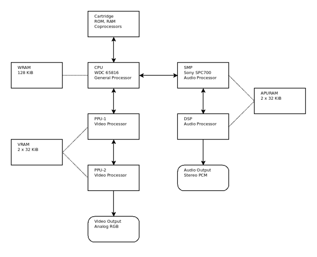
Let's start by taking a look at the components that make up the SNES:

The arrows indicate the direction that the various processors in the SNES can communicate with one another, and the dotted lines represent memory chip connections.
The key thing to take away right now is to note that the video and audio output are sent directly from the PPU and DSP specifically. That means they function like “black boxes” where we don’t have any visibility into what happens inside. This will be important later on.
Correctness
Imagine you are emulating a CPU's "multiply" instruction, which takes two registers (variables), multiplies them together, and produces a result and some flags that represent the status of the result (such as overflow).
We could devise a software program that multiplies every possible value from 0 to 255 as both the multiplier and multiplicand. Then we could output both the numeric and flag results of the multiplication. This would produce two 65,536-entry tables.
By analyzing these tables, we could determine exactly how and when the CPU results were set certain ways. Then we could modify our emulators so, when running the same test, we produce exactly the same tables at the same times.
Now let's say the CPU had 16-bit x 16-bit multiplications. Testing every possible value would generate 4 billion results, which is starting to push what is practical to test in a reasonable amount of time. If the CPU had 32-bit x 32-bit multiplications, it wouldn’t be practical to test all combinations of inputs before the heat death of the universe (with current technology, at least).
In cases like this, we would have to get more selective with our tests and try to determine exactly when flags might change, when results might overflow, and so forth. Otherwise we'd have tests that would never complete.
Multiplication is a fairly trivial operation, but this is the general process behind reverse engineering, and it extends to more complex operations such as how the SNES' horizontal blanking DMA (direct memory access) transfers work. We create tests that try to detect what happens on edge cases, then confirm that our emulation behaves identically to a real SNES.
Oscillators and cycles
The SNES contains two oscillators: a crystal clock that runs at ~21MHz, which controls the CPU and PPUs; and a ceramic resonator that runs at ~24MHz, which controls the SMP and DSP. Cartridge coprocessors will sometimes use the ~21MHz CPU oscillator and sometimes include their own oscillators that run at different frequencies.

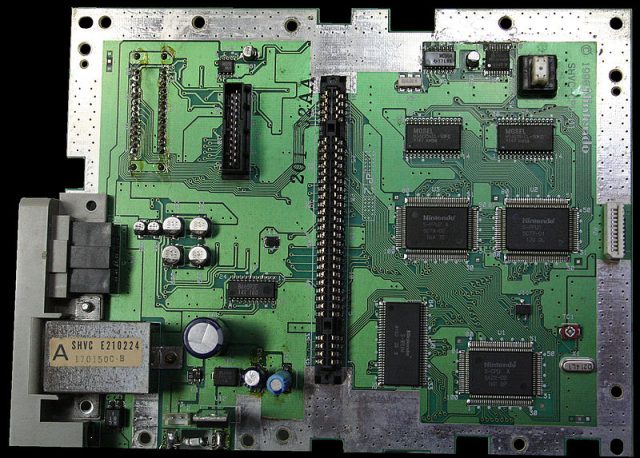
Recreating this original Super Famicom circuit board purely in software is harder than it looks.
A clock is the core timing element of any system, and the SNES is designed to perform various tasks at certain frequencies and times.
If you imagine a 100Hz clock, it is a device with a digital pin that transitions to logic high (+5 volts, for instance), and then back to logic low (0 volts, or ground) 100 times per second. So every second, the pin voltage will fluctuate 200 times total: 100 rising clock edges and 100 falling clock edges.
A clock cycle is generally treated as one full transition, so a 100Hz clock would generate 100 clock cycles per second. There are some systems that require distinguishing between rising and falling edges, and for those, we break this further down into half-cycles to denote each phase (high or low) of the clock signal.
The key goal of an authentic emulator is to perform tasks in exactly the same ways and at exactly the same times as the real hardware. It doesn't much matter specifically how the tasks are performed. All that matters is that the emulator, when given the same inputs, generates the same outputs with the same timing as real hardware.
Timing
Sometimes, operations happen over time. Take SNES CPU multiplication, for instance. Rather than pausing to wait for multiplication to complete, the SNES CPU calculates the multiplication result one bit at a time in the background over eight CPU opcode cycles. This allows your code to possibly do other things while waiting on the multiplication to complete.
Any commercially released software is likely to wait those eight cycles, because if you try to read the result before it's ready, you will get a partially computed result instead. Yet earlier SNES emulators gave correct results immediately, without waiting these extra cycles.
When hobbyists started creating and testing homebrew software via emulators, this discrepancy started to cause some problems. Some of this software, such as many early Super Mario World ROM hacks, only worked correctly on these earlier emulators, and not on real SNES hardware. That's because they were designed with the emulator's immediate (and inauthentic-to-real-hardware) multiplication results in mind.
As emulators improved, this old software broke, and we have had to subsequently offer compatibility options in our newer emulators in order to not lose this software to time. Yes, as surreal as it is to say, these days our emulators have to emulate other emulators! How meta!
The nice thing about the CPU multiplication delay is that it's very predictable: the eight computation cycles start immediately after requesting a multiplication. By writing code to read the results after every cycle, we were able to confirm that the SNES CPU was using the Booth algorithm for multiplication.
Clock Synchronization
Other operations are not so simple to model, since they happen asynchronously in the background. The SNES CPU's DRAM refresh is one such case.
During the rendering of every scanline, at a certain point, the entire SNES CPU freezes for a short duration as the contents of the RAM chip are refreshed. This is needed because, as a cost-cutting measure, the SNES used dynamic RAM (rather than static RAM) for its main CPU memory. Dynamic RAM must be periodically refreshed in order to preserve its contents over time.

For a truly perfect emulator, just making ~3,500 commercially released SNES games playable isn't enough. Every function of the system has to be simulated with cycle-perfect accuracy, too.
The key insight to figuring out the precise timing of these operations was to take advantage of the SNES PPU’s horizontal and vertical counters. These counters advance and are reset after each horizontal and vertical blanking period. However, their precision is only a quarter of the SNES' CPU oscillator frequency; that is to say, the horizontal counter increments only once every four clock cycles.
By reading the counters multiple times, I was able to determine which quarter of a clock cycle the counter was aligned with. By combining that insight with a specially crafted function that could step by a precise, user-specified number of clock cycles, it became possible to perfectly align the SNES CPU to any exact clock cycle position I wanted.
By iterating over a range of clock cycles in a loop, I could determine exactly when certain operations (such as DRAM refresh, HDMA transfers, interrupt polling, etc.) would occur, and I was able to reproduce this precisely under emulation.
The SNES SMP chip has its own timers as well, and similar reverse engineering was successful against that processor as well. I could spend an entire article talking about the SMP TEST register alone, which allows coders to control the clock divider of the SMP and its timers, among other horrible things. Suffice it to say that, while it was not an easy or fast process, we were ultimately victorious.
Collecting coprocessors

The SuperFX chip is just one of many cartridge coprocessors that an SNES emulator has to handle correctly.
That means an SNES emulator needs to be able to handle the instruction and pixel caches of the SuperFX; the memory bus conflict arbitrator of the SA-1 (which allowed the SNES CPU and SA-1 to share the same ROM and RAM chips simultaneously); the embedded firmware of the DSP-1 and Cx4; the prediction-based arithmetic coders of the S-DD1 and SPC7110; and the odd BCD (binary-coded decimal) edge cases of the real-time clocks. Slowly but surely, by applying the above techniques to determine correctness and timing, we were able to near-perfectly emulate all of these chips.
It actually took a massive effort and thousands of dollars to decap and extract the programming firmware from the digital signal processors used in various games. In one instance, emulation of the NEC uPD772x led to code from higan being used to save the late professor Stephen Hawking's voice!
In another case, we had to reverse-engineer the entire instruction set of the Hitachi HG51B architecture, because this architecture was never publicly documented. In yet another, one game (Hayazashi Nidan Morita Shougi 2) ended up containing a full-blown 32-bit, 21MHz ARM6 CPU to accelerate its Japanese chess engine!
Preserving all of the SNES coprocessors alone was a multi-year journey full of challenges and surprises.
Processing digital signal
Not to be confused with the DSP-1 cartridge coprocessor, the Sony S-DSP (digital signal processor) chip is what generated the distinctive sound from the SNES. This chip combined eight voice channels with 4-bit ADPCM encoding to produce a 16-bit stereo signal.
On the surface, and per the system diagram from earlier, the DSP initially looks like a black box: you configure the voice channels and mixer settings and sit back as it generates sound to be sent to your speakers.
But one key feature allowed a developer by the name of blargg to fully reverse-engineer this chip: the echo buffer. The SNES DSP has a feature that mixes the outputs from previous samples together to produce an echo effect. This happens at the very end of the audio generation process (aside from one last final mute flag that can be applied to silence all audio output.)
By writing carefully cycle-timed code and monitoring those echo results, it became possible to discover the exact order of operations the SNES DSP would take to generate each sample and to produce cycle-accurate, bit-perfect audio.
from Hacker News https://ift.tt/39whL1x
No comments:
Post a Comment
Note: Only a member of this blog may post a comment.